Last week I heard about the Indian Cabinet approving the proposal for setting up of two Fabs in India. One led by IBM, Tower Jazzand JP Associates(an Indian business house), and the other led by HSMC(Hindustan Semiconductor Manufacturing Co.), ST Microelectronicsand Silterra. Indian Semiconductor community including IESA… Read More
 CEO Interview with Dave Kelf, CEO of Breker Verification SystemsIn the functional verification space, Breker Verification Systems stands…Read More
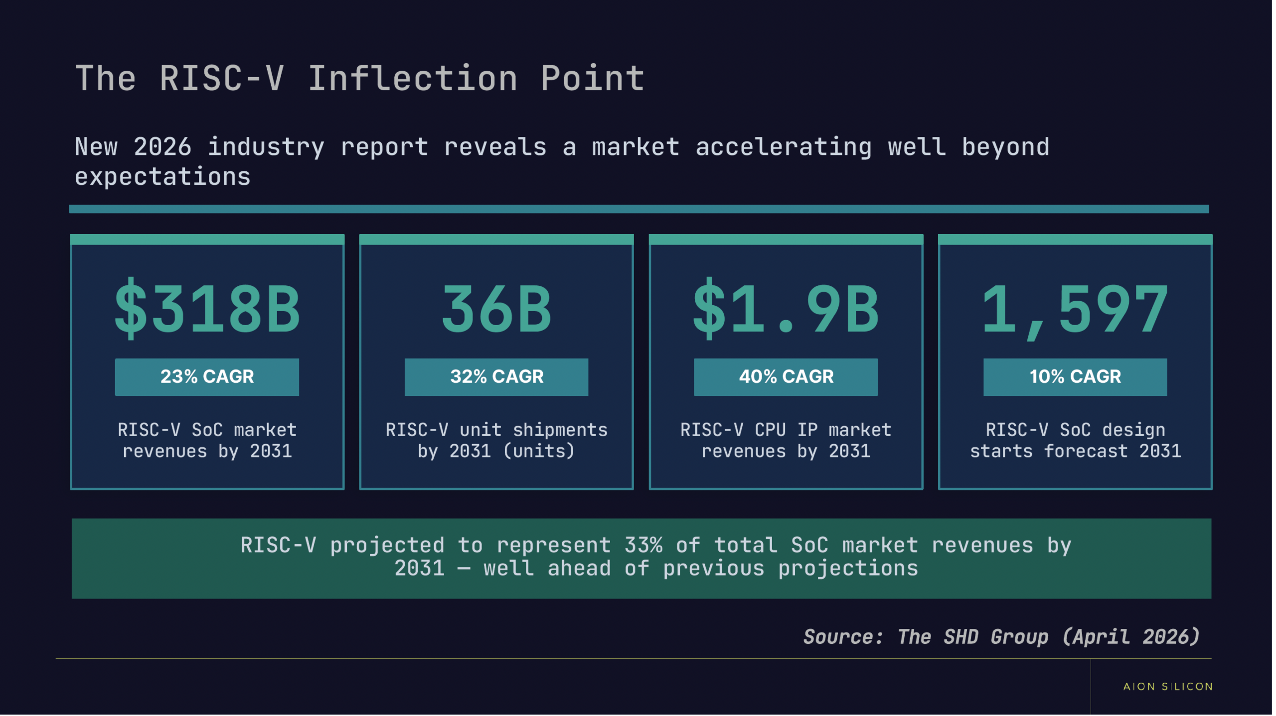 RISC-V: From Niche Architecture to Strategic FoundationAt the recent RISC-V Now by Andes conference,…Read More
 Bringing mathematical rigour in the world of hardware - a journey into Formal VerificationThis interview presents the first steps of Robert…Read More
 The Great Divide: A Tale of Three Hardware Emulation ArchitecturesHardware emulation arose as a necessity out of…Read More
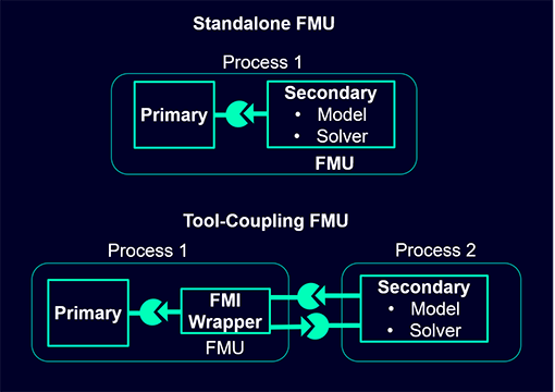 A Different Angle on Co-Simulation for SystemsCo-simulation, two or more simulations running concurrently in…Read More
Sidense and TSMC Processes
I’ve written before about the basic capabilities of Sidense’s single transistor one-time programmable memory products (1T-OTP). Just to summarize, it is an anti-fuse device that works by permanently rupturing the gate oxide under the bit-cells storage transistor, something that is obviously irreversible.… Read More
Back To The Future: 50th Anniversary of EDA
October 16[SUP]th[/SUP] at the Computer History Museum, EDAC is hosting EDA: Back to the Future to celebrate 50 years of EDA. EDAC always has a fall event of some sort and historically it has been the Kaufman Award Dinner. This year, the Kaufman Award was presented (to Chenming Hu) at 50[SUP]th[/SUP] DAC, so the fall EDAC calendar… Read More
Analog Characterization Environment (ACE)
I’m looking forward to the 2013 TSMC Open Innovation Platform Ecosystem Forum to be held Oct. 1[SUP]st[/SUP] in San Jose. One paper in particular that has my attention is titled, “An Efficient and Accurate Sign-Off Simulation Methodology for High-Performance CMOS Image Sensors,” by Berkeley Design Automation & … Read More
The Significance of Apple’s 64 Bit A7
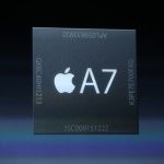
The disappointment amongst analysts is palpable. Dreams of low cost iphones for the masses were kicked away when Apple introduced their two new iphones at the same price points as the old ones. Clearly Apple is playing a different game than what most others are anticipating as the market runs to 5BU. The market has split into the land… Read More
Emerging Trend – Choose DRAM as per Your Design Need
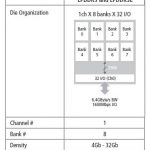
Lately I was studying about new innovations in memory world such as ReRAM and Memristor. As DRAM (although it has become a commodity) has found its extensive use in mobile, PC, tablet and so on, that was an inclination too to know more about. While reviewing Cadence’s offering in memory subsystems, I came across this whitepaperwhich… Read More
Breaking news: Microsoft acquires Apple!
Despite the relative success of their latest smartphone, iPhone15s, the Cupertino firm had never been able to renew with the success of legendary iPhone5s, launched ten years ago, in 2011. As of today, we don’t know if Microsoft will keep iPhone and iPad product lines, or decide to provide these with a lethal injection…
Some history:… Read More
Intel Quark: Synthesizable Core?
At IDF Brian Krzanich gave the keynote. I won’t summarize the whole thing here but just talk about one part that was something they had actually managed to keep secret ahead of time: Quark.
Quark is a synthesizable core. It uses 1/10th power of Atom and is 1/5 size. Now I am writing this, I don’t know if this is a fair comparison… Read More
GlobalFoundries Expands in Singapore
GlobalFoundries has been in Singapore for a long time. Longer than GlobalFoundries has existed in fact. Chartered Semiconductor was started in Singapore in 1987 and GF acquired them in early 2010 less than a year after they were created by spinning out the manufacturing arm of AMD. When GF was started their state of the art fab was… Read More
Cadence Introduces Palladium XP II
Well, despite all the arguments in the blogosphere about what process node palladium’s silicon is, and whether the design team is competent, and why it reports into sales…Cadence has announced their latest big revision of Palladium. Someone seems to be able to get things done. Of course it is bigger and faster and … Read More






The Semiconductor Growth Numbers are Insane but the Real World Doesn’t Tally!