In this pretty shaky NVM IP market, where articles frequently mention legal battles rather than product features, it seems interesting to take a look at this Newsletter from Novocell Semiconductor starting with these words: “As the Christmas carols and festive music floods the airwaves (and the shopping areas) here in western Pennsylvania and the threat of cold and snow looms, the cheery band of engineers at Novocell are finding themselves overcome with the holiday spirit…”

This is a nice way to start a Newsletter, but you also can find some post about very interesting topics. Like this one about the legacy nodes, where we can discover that customer project increase at nodes from 90nm and above:
Rumors of the demise of legacy nodes have been greatly exaggerated;
2012 customer project work and interest increases at nodes from 90nm to 350nm!
During the past 6 months, we have been seeing a noticeable increase in inquiries, quotes, and project wins for customer projects at nodes from 130nm, 180nm, 250nm and that old standby, 350nm.
Reading the industry press would give the impression that the world has moved to 28 and 40nm processes, and that a vast majority of the microelectronics/SoC industry is preparing to rollout on 20nm next year and on 14nm finFET as soon as TSMC’s new plant doors open in 2015…
… to be continued in the newsletter

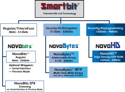
If you didn’t knew, you will learn why Novocell’s Smartbit-family of OTP, the only anti-fuse vendor providing OTP at the larger process nodes, provides the highest level of foundry and process independence available.
Very interesting to notice, Novocell has decided to propose a new type of license, that you usually would see in the Software of RTL IP market:
Novocell introduces new “Evaluation Period” License
As more and more firms have come knocking to inquire about antifuse OTP in general, and advantages of our unique Smartbit technology in specific, we have encountered a large number of firms who have had experience with EEPROM and conventional ROM, but have not worked with memory quite like ours.

Perhaps like you, they are used to getting surprises downstream in projects: additional chip area needs for redundant bits and error correction circuitry based on reliability requirements; Or they commonly have been burned by other technologies’ integration difficulties or late-breaking news of needs for charge pumps, control circuitry, or other “gotcha’s”.

To help ease these concerns, Novocell has introduced an Evaluation License, that provides your team from 6-9 months to evaluate the Novocell IP macro of interest at a cost reduced to cover support and IP updates, and allows for conversion to a standard IP license upon move to production.
Did you know that Novocell had close a strong technology partnership with major silicon foundries, like IBM, and that Novocell has completed the final validation step and has been approved as a IBM Foundry Business Partner, along with recognition of the foundational Novobits OTPproduct line as a Ready for IBM Technology?
Then, You should have a look at the newsletter!
Eric Esteve from IPNEST –


Is Intel About to Take Flight?