Yesterday evening was EDAC’s first mixer. I assume the first of a regular event. It was held in Mountain View in the old train station which is now the Savvy Cellar wine bar. I had a nice glass of rosé from Provence that reminded me of the years that I lived in the south of France. Some of the money we spent went to charity, to the Mountain… Read More
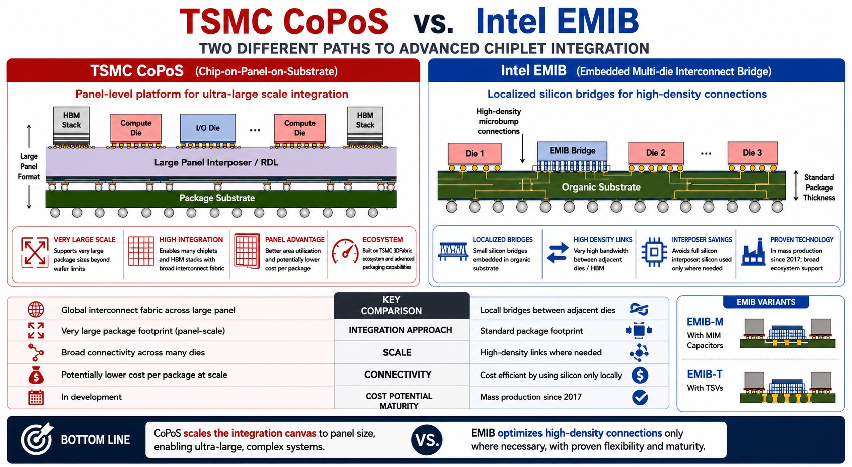 TSMC CoPoS Versus Intel EMIB Semiconductor PackagingTSMC’s CoPoS, generally described as Chip-on-Panel-on-Substrate, and Intel’s…Read More
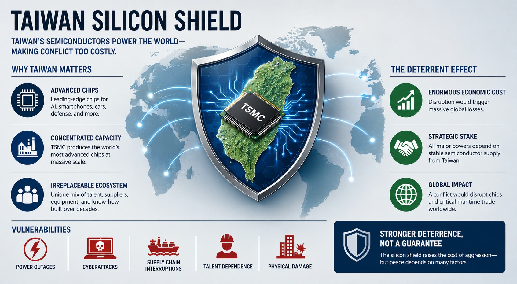 The Silicon Shield Has Never Been Stronger!The “Silicon Shield” describes the idea that Taiwan’s…Read More
 Agentrys Designs a Real Chip with its Multi-Agent WorkforceThe face of EDA is changing. For forty…Read More
 Must-See DAC Panel – Build vs Buy: Who Owns the Intelligence Behind Tomorrow's Chips?This year, DAC will be buzzing about AI…Read More
Mixed-Signal SoC Debugging & IP Integration Made Easy
A semiconductor SoC design can have multiple components at different levels of abstractions from different sources and in different languages. While designing an SoC, IPs at different levels have to be integrated without losing the overall design goals. Of course, quality of an IP inside and outside of an SoC must be tested thoroughly.… Read More
SmartConnect goes five by five for the IoT
OK, enough with octa-core mobile monstrosities for now. Let’s shift gears to Embedded World 2014 and the lower end of the spectrum, one that will make up the vast majority of devices on the Internet of Things: tiny, low power microcontrollers with integrated wireless connectivity.
There still seems to be some stigma about putting… Read More
Celebrating 50 Billion ARM Powered Chips!
In case you have not seen it yet there is a website named 50BillionChips where you can follow the journey of ARM. This goes quite well with the brief history of ARM we wrote last year in preparation for our bookFabless: The Transformation of the Semiconductor Industry. ARM was a big part of that transformation of course.… Read More
A Brief History of STMicroelectronics
STMicroelectronics is the result of the 1987 marriage between famed semiconductor companies SGS Microelettronica of Italy and Thomson-CSF Semiconductor of France. You may recognize the name SGS-Thomson which was replaced by STMicroelectronics in 1998. After the merger SGS-Thomson was ranked as number 14 in the top 20 semiconductor… Read More
Yamaha Selecting Audio/Voice DSP Architecture?
…or Chongquing CYIT Communication Technology Co Ltd. Both of them have recently licensed the CEVA-TeakLite-4 DSP, the latest for its multi-mode wireless baseband chips targeting 4G terminals, including smartphones and tablets (CYIT) and Yamaha to address the need to run increasingly complex voice pre-processing algorithms,… Read More
IoT: the sum of all technology opportunities
There was a time not that long ago, before smartphones arrived on the scene, where Mentor Embedded Nucleus RTOS was dominant in non-Nokia feature phones – Mentor is part of the “Billion Unit Mobile Club”. Since then, Mentor has been searching to recreate that type of success, and like so many other software firms, they are now aiming… Read More
TI’s Way of Strategies – Formation & Execution
For a company to stand still and continually prosper even after facing several downturns in its career of 80+ years, and still move swiftly with strong commitment and confidence, its strategy has to be right and rock solid possessing sustainable competitive advantage, and of course it has to be an early mover in everything it does… Read More
A Brief History of Chip Design at Apple Computer
Steve Wozniak in 1976 designed the Apple 1 while working at HP during the daytime, and he used standard parts to keep costs low, like:
- 6502 CPU from MOS Technology
- 8K of DRAM
- TTL logic for driving video and random logic
- PROM to hold the BASIC language and primitive OS
Getting an MPW Quote on My iPhone
As I blogged about recently, eSilicon have completely automated the quote process for their MPW shuttle service. You can use an online interface that runs in the browser but there is also an app that you can download from the App Store.
So I decided I had a few million dollars to burn and I’d get myself my very own TSMC 20nm parts.… Read More
Enhancing Multi-Domain System Simulation with FMI Co-Simulation