You are currently viewing SemiWiki as a guest which gives you limited access to the site. To view blog comments and experience other SemiWiki features you must be a registered member. Registration is fast, simple, and absolutely free so please,
join our community today!
Posts Search Results for "3dblox"
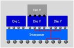
2.5D and 3D ICs present special challenges since these designs contain multiple chiplets of different materials integrated in all three dimensions. This complexity demands full assembly verification of the entire stack, considering all the subtle electrical and physical interactions of the complete system. Identifying… Read More
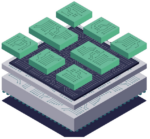
The next design revolution is clearly upon us. Traditional Moore’s Law is slowing, but the exponential demand for innovation and form factor density is not. When you can no longer get it done with a single monolithic chip, moving to a multi-die approach is the answer. This emerging design methodology has many challenges – supply… Read More
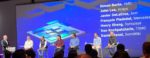
As the focal point of the TSMC OIP ecosystem, TSMC has been driving important initiatives over the last few years to bring multi-die systems to the mainstream. As the world is moving quickly toward Generative AI technology and AI-based systems, multi-die and chiplet-based implementations are becoming essential. TSMC recently… Read More
The 15th TSMC Open Innovation Platform® (OIP) was held last week. In preparation we did a podcast with one of the original members of the TSMC OIP team Dan Kochpatcharin. Dan and I talked about the early days before OIP when we did reference flows together. Around 20 years ago I did a career pivot and focused on Strategic Foundry Relationships.… Read More
For many years, monolithic chips defined semiconductor innovation. New microprocessors defined new markets, as did new graphics processors, and cell-phone chips. Getting to the next node was the goal, and when the foundry shipped a working part victory was declared. As we know, this is changing. Semiconductor innovation is… Read More
At the recent Synopsys Users Group Meeting (SNUG) I had the honor of leading a panel of experts on the topic of chiplets. One of those panelists was the very personable Dr. Henry Sheng, Group Director of R&D in the EDA Group at Synopsys. Henry currently leads engineering for 3DIC, advanced technology and visualization.
Are we
…
Read More
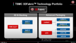
TSMC’s 3DFabric initiative was a big focus at the symposium, as it should be. I remember when TSMC first went public with CoWos the semiconductor ecosystem, including yours truly, let out a collective sigh wondering why TSMC is venturing into the comparatively low margin world of packaging. Now we know why and it is absolutely… Read More
At SemiWiki we’ve written four times now about how TSMC is standardizing on a 3DIC physical flow with their approach called 3Dblox, so I watched a presentation from John Ferguson of Siemens EDA to see how their tool flow supports this with the Calibre tools. With a chiplet-based packaging flow there are new physical verification… Read More
If, like me, you’ve been paying too little attention to historically less glamorous areas of chip design like packaging, you’ll wake up one day and realize just how much things have changed and continue to advance and how interesting it’s become.
One of the main drivers here is the increasing use of chiplets to counter the decreasing… Read More
On November 10th I watched the presentation by L.C. Lu, TSMC Fellow & VP, as he talked about enabling system innovation with dozens of slides in just 26 minutes. TSMC is the number one semiconductor foundry in the world, and their Open Innovation Platform (OIP) events are popular and well attended as the process technology and… Read More


TSMC N3 Process Technology Wiki