Electron beam lithography is commercially used to directly write submicron patterns onto advanced node masks. With the advent of EUV masks and nanometer-scale NIL (nanoimprint lithography), multi-beam writers are now being used, compensating the ultralow throughput of a single high-resolution electron beam with the use of over 100,000 beams [1-2]. Unlike optical or EUV scanners, the resolution is not determined by the numerical aperture (NA) of the system. Instead, it starts with how small the electron beam is focused, followed by how the electrons are subsequently scattered and release more electrons which are subsequently scattered.
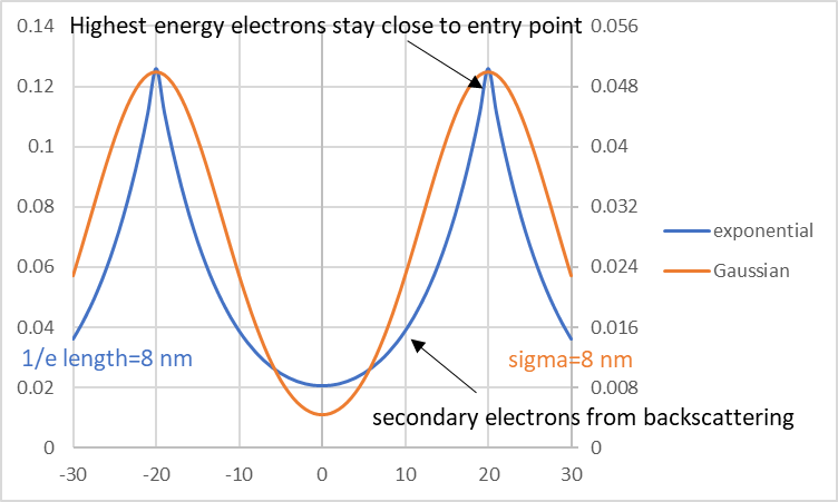
Commonly, Gaussian functions are used to model the electron beam and scattering profiles. However, a single Gaussian function is not sufficient to build the effective point spread function. This is because the backscattered electrons travel far beyond the range of the immediately scattered electrons. At least two Gaussian functions (and generally more) are needed for an accurate profile. Some published results from the literature [3-4], in fact, indicate exponential functions as more appropriate for fitting the energy deposited by a high-energy electron beam. Compared to a Gaussian function, an exponential function has a sharper, narrower peak, a sharper drop-off, and a more extended tail.

Figure 1. Exponential functions more realistically describe the combination of a narrow beam with extended backscattering.
The narrow peak and sharp drop-off are consistent with the highest energy electrons (>>10 keV) not deviating far laterally from the entry point, while the extended tail comes from all the secondary electrons (many generations, no doubt) from electrons which are backscattered from the substrate.
The resolution limit from this point spread function can be studied (as in the optical cases) by considering the space between two exposed points. As may be expected, the shot noise from the electron dose plays a critical role (Figure 2).

Figure 2. Reducing the dose to 16% of the nominal value increases the impact from shot noise visibly. The two exposed spots here are separated by 40 nm. The number of Poisson events is considered proportional to the exponential deposited energy profile.
What also should not be a surprise is the impact of blur. Here blur comes from a wider range of electron energies (many keVs) than expected from EUV lithography (only up to ~92 eV).

Figure 3. Increasing blur reduces the peak-valley dose difference. Since the peak dose here is fixed, the valley dose is actually increasing with blur. As in Figure 2, the two exposed spots here are separated by 40 nm, and the number of Poisson events is considered proportional to the exponential deposited energy profile.
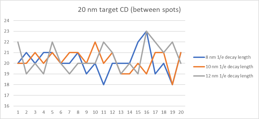
From Figure 3, we note two trends. First, the peak-valley dose difference diminished with increasing blur. Second, while the peak dose is fixed, the valley dose is increasing with increasing blur. In terms of the impact on stochastic dose variations, these two trends counter each other. The first trend increases sensitivity to fluctuations, but the second trend reduces the amplitude of such fluctuations in accordance with Poisson statistics. Consequently, the CD variation due to these fluctuations is comparable among the three cases (Figure 4).

Figure 4. CD variation for 20 points repeatability run, for the cases shown in Figure 3. The amount of variation is comparable among the three cases.
The 3 sigma uniformity is on the order of 3-4 nm (~15-20%) for the three cases examined. Obviously, the dose needs to be increased to reduce this to smaller values. However, this will proportionally increase write time if beam number is not increased; a doubling is considered unacceptable [2]. Larger CDs (>20 nm) will not be impacted as significantly [5], as the peak-valley difference is increased and more point spread functions are overlapped together in writing the spots [1,6]. However, for nanoimprint masks and High-NA EUV masks with subresolution assist features (SRAFs), the stochastic variations cannot be ignored.
References
[1] M. Tomandl et al., Proc. SPIE 12802, 1280204 (2023).
[2] C. Klein et al., Proc. SPIE PC12497, PC1249707 (2023).
[3] V. R. Manfrinato et al., Nano. Lett. 14, 4406 (2014).
[4] V. R. Manfrinato et al., Nano. Lett. 13, 1555 (2013).
[5] K. Ichimura et al., Proc. SPIE 12293, 122930Q (2022).
[6] K. Ichimura et al., Proc. SPIE 10584, 105840P (2018).
This article first appeared on LinkedIn Pulse: The Significance of Point Spread Functions with Stochastic Behavior in Electron-Beam Lithography
Also Read:
KLAC- OK quarter in ugly environment- Big China $ – Little Process $ – Legacy good
ASML- Longer Deeper Downcycle finally hits lithography – Flat 2024 – Weak Memory – Bottom?
ASML- Absolutely Solid Monopoly in Lithography- Ignoring hysteria & stupidity
Share this post via:


Captain America: Can Elon Musk Save America’s Chip Manufacturing Industry?