You are currently viewing SemiWiki as a guest which gives you limited access to the site. To view blog comments and experience other SemiWiki features you must be a registered member. Registration is fast, simple, and absolutely free so please,
join our community today!
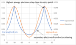
Electron beam lithography is commercially used to directly write submicron patterns onto advanced node masks. With the advent of EUV masks and nanometer-scale NIL (nanoimprint lithography), multi-beam writers are now being used, compensating the ultralow throughput of a single high-resolution electron beam with the use… Read More
Cutting the Key to 14nm Lithographyby Beth Martin on 04-08-2013 at 2:30 pmCategories: EDA, Siemens EDA
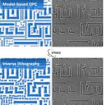
It appears that immersion lithography is now the plan of record for manufacturing ICs at 14nm. How is it possible to use 193nm wavelength light at 14nm? How can we provide the process window to pattern the such tight pitches? The secret lies in computational lithography. For 20nm, the two key innovations in computational lithography… Read More
The industry plans to use 193nm light at the 20nm, 14nm, and 10nm nodes. Amazing, no? There is no magic wand; scientists have been hard at work developing computational lithography techniques that can pull one more rabbit out of the optical lithography hat.
Tortured metaphors aside, the goal for the post-tapeout flow is the same… Read More