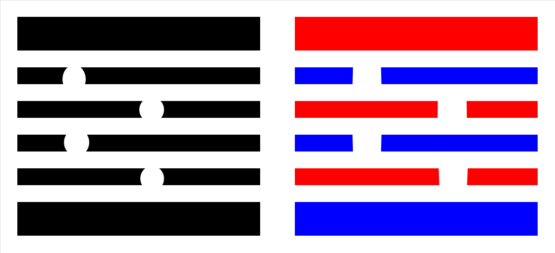
The 5nm foundry node saw the arrival of 6-track standard cells with four narrow routing tracks between wide power/ground rails (Figure 1a), with minimum pitches of around 30 nm [1]. The routing tracks require cuts [2] with widths comparable to the minimum half-pitch, to enable the via connections to the next metal layer with the same minimum pitch. In order to achieve this reliably, it becomes necessary to have alternate lines made of different materials (Figure 1b) that can be selectively etched with different etch chemistry [3,4], for example, silicon nitride and spin-on carbon. In this way, etch pitch is effectively doubled from the target metal pitch. This has some beneficial impact on the lithography.

Figure 1 (a) Left: Four narrow routing lines between wider power/GND rail lines. (b) Right: Alternating lines should be constructed from materials that are etched by selective chemistry so that cut lines can cross over intervening lines without affecting them.
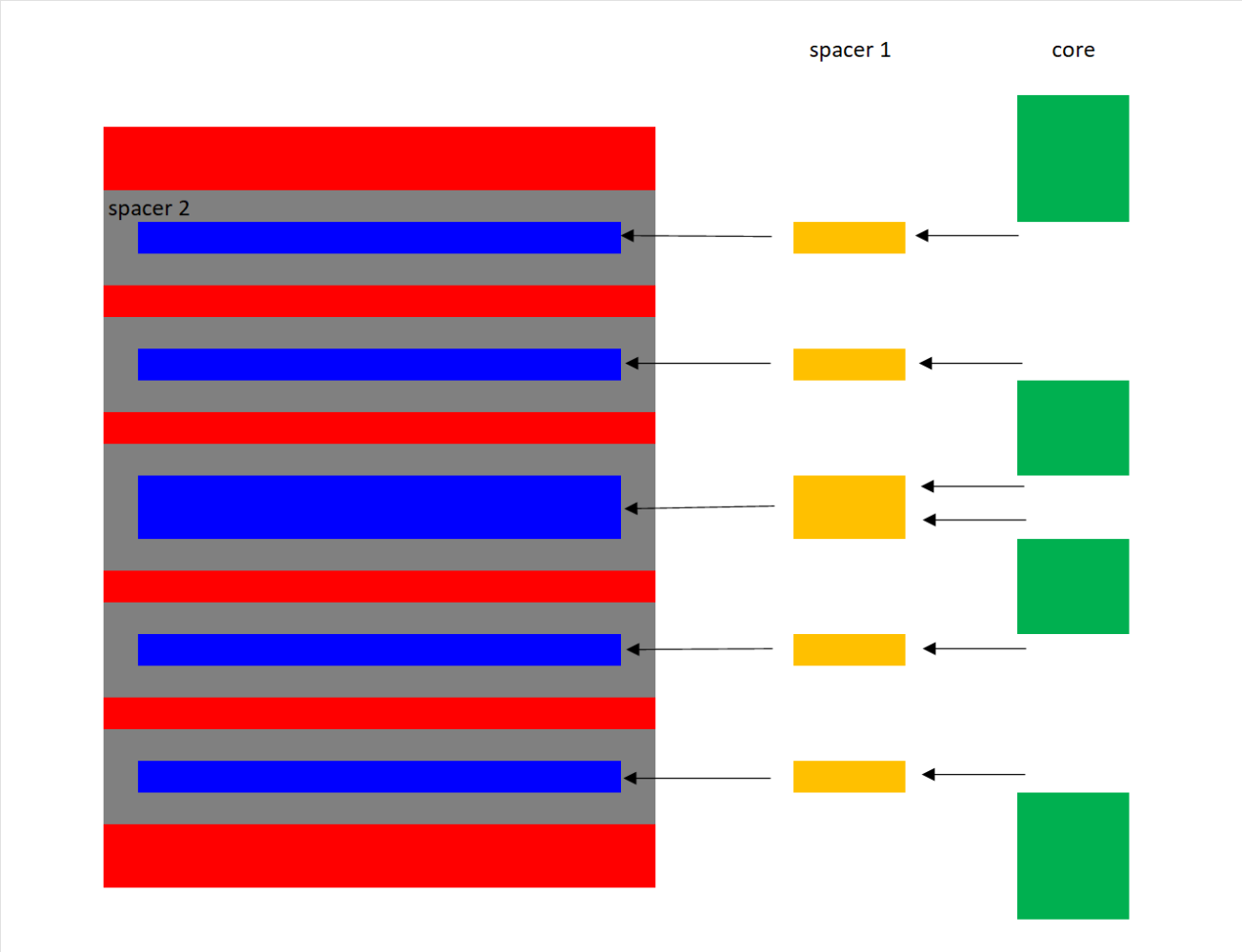
Producing this series of lines is possible by use of SAQP (Self-Aligned Quadruple Patterning), as detailed in Figure 2. To target a 30 nm final pitch, the starting core pitch for SAQP would be 120 nm which is a comfortably manageable pitch for a leading edge immersion tool (193 nm wavelength, 1.35 NA). This approach can be foreseeably extended down to 20 nm minimum track pitch.

Figure 2. SAQP with a starting core pattern (green) that will result in alternating material tracks. The blue lines are defined by the first spacers (yellow), while the red lines are defined by the material that fills the gaps after the second spacers (gray) are formed. Note the merger of the first spacers in the middle of the pitch.
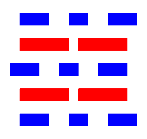
The alternating material line arrangement can also be extended to include SRAM patterning (Figure 3) [5].

Figure 3. Alternating material line arrangement for an SRAM M0 layer example [5].
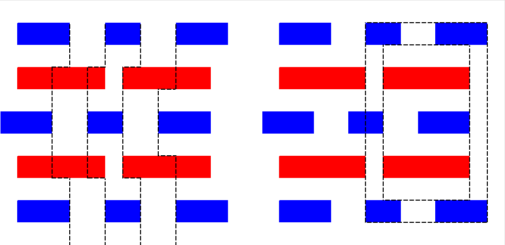
The cuts for the lines shown in the above figures are achieved in two steps, requiring two masks, one for cutting the blue lines (not affecting the red lines), the other for cutting the red lines (not affecting the blue lines). The spaces between cuts may be narrow enough to warrant double patterning without EUV as well. Self-aligned double patterning (SADP) is the preferred approach [6]. Figure 4 shows the outlines of the SADP cut patterns for the case of Figure 3.

Figure 4. Crossing SADP patterns for line cuts for the pattern of Figure 3.
Since the two-material line arrangement is necessary for the reliable line cutting in and of itself, this minimum three-mask approach (SADP or SAQP, blue line cut, red line cut) would also be required for EUV, not just DUV. Regarding via patterning, in a trench-first, via-last dual-damascene scheme [4,7], self-aligned vias would only require one DUV mask (possibly with SADP), while making use of the prior multipatterned metal trench line pattern. Thus, we see that enforcing cut-friendly layouts leads to an unexpectedly wavelength-agnostic outcome, at least as far as mask count is concerned. In light of the difficulty of getting hold of an EUV tool these days, this is indeed a welcome scenario.
References
[1] J. U. Lee et al., “SAQP spacer merge and EUV self-aligned block decomposition at 28 nm metal pitch on imec 7nm node,” Proc. SPIE 10962, 109620N (2019).
[2] W. Gillijns et al., “Impact of a SADP flow on the design and process for N10/N7 Metal layers,” Proc. SPIE 9427, 942709 (2015).
[3] F. Lazzarino et al., “Self-aligned block technology: a step toward further scaling,” Proc. SPIE 10149, 1014908 (2017).
[4] B. Vincent et al., “Self-aligned block and fully self-aligned via for iN5 metal 2 self-aligned quadruple patterning,” Proc. SPIE 10583, 105830W (2018).
[5] S. Sakhare et al., “Layout optimization and trade-off between 193i and EUV-based patterning for SRAM cells to improve performance and process variability at 7nm technology node,” Proc. SPIE 9427, 94260O (2015).
[6] K. Oyama et al., “The enhanced photoresist shrink process technique toward 22nm node,” Proc. SPIE 7972, 79722Q (2011).
[7] H. Tomizawa et al., “Robust Self-Aligned Via Process for 64nm Pitch Dual-Damascene Interconnects using Pitch Split Double Exposure Patterning Scheme,” 2011 IITC.
This article originally appeared in LinkedIn Pulse: Etch Pitch Doubling Requirement for Cut-Friendly Track Metal Layouts: Escaping Lithography Wavelength Dependence
Pattern Shifts Induced by Dipole-Illuminated EUV Masks
Revisiting EUV Lithography: Post-Blur Stochastic Distributions
Share this post via:


Musk’s Orbital Compute Vision: TERAFAB and the End of the Terrestrial Data Center