For advanced lithography used to shrink semiconductor device features according to Moore’s Law, resolution limits are an obvious consideration. It is often perceived that the resolution limit is simply derived from a well-defined equation, but nothing can be further from the truth.
Optical Lithography: the fine print of the Abbe criterion
The “brick wall” resolution limit of an optical lithography system is the Abbe criterion recited as a formula: minimum half-pitch = 0.25 wavelength/(numerical aperture) [1]. In reality, though, the resolution limit is actually far more complex – it depends on the illumination direction. For on-axis illumination, with light only at the center of the pupil, the minimum pitch is wavelength/(numerical aperture). For lines in the plane of incidence, an incident angle corresponding to the numerical aperture (the maximum angle) in the wafer plane produces no image, whereas the same angle in the plane of incidence perpendicular to the lines gives a minimum pitch of 0.5 wavelength/(numerical aperture); this is the origin of the recited Abbe formula.
Post-optical lithography, such as EUV (extreme ultraviolet) and electron-beam lithography, is subject to several additional constraints on resolution.
Secondary electrons
As ionizing radiation, EUV, X-rays, electron beams, and ion beams all produce secondary electrons released from atoms. These electrons then move around, blurring the image. 15 nm half-pitch zones by electron-beam exposure of PMMA required double patterning, even for a 6.5 nm diameter 100keV electron beam [2]. Nanoimprint templates with 14 nm half-pitch also required double patterning using spacers [3]. Low-energy electron exposures indicate 20 nm thick resist may be patterned even with 2 eV electrons [4]. Thus, we expect secondary electron range to reach 20 nm, especially with higher doses. These higher doses are necessary to address stochastic defects.
Stochastic defects
Stochastic defects have recently been observed with some EUV studies[5,6]. It is believed to be generally applicable when shot noise affects the resist exposure, i.e., dose is too low. Thus, electron beam lithography is also likely to experience shot noise and stochastic defects [7]. Optical lithography doses, on the other hand, are generally well over the levels where shot noise would be a concern. Secondary electrons also can contribute to stochastic defects [8,9]. In relatively high volume, 5nm (5LPE) layouts are susceptible to stochastic defects [10]; these are expected to be 36 nm metal pitch (18 nm half-pitch) [11].
EUV thick mask effects
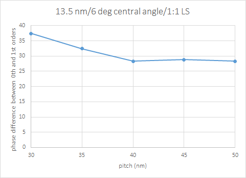
EUV specifically uses optically thick reflective multilayer masks, i.e., the 13.2-13.8 nm wavelength range light passes through a series of 80 alternating Si/Mo layers extending over many wavelengths. For a given angle of incidence q, the path covered by reflection from a given depth in the multilayer is proportional to cos(q). In radians, q can be expressed as 0.105 (1+a), with 0.105 representing the 6 degree central ray angle and a<<1. cos(q) can then be estimated by the Taylor approximation as 0.01 (1+0.5 a). It turns out a is inversely proportional to line pitch, for the optimum illumination (sine(angle) = 1/2 wavelength/ pitch). As a result, the phase difference between the 0th (a=0) and 1st (a=1/8 wavelength/pitch) orders used to form the image will increase dramatically as pitch decreases (lines perpendicular to plane of incidence), as shown in Figure 1 [12]. This phase difference has two detrimental effects: (1) best focus dependence on pitch, and (2) loss of image contrast (less sharp edge) at smaller pitches. Referring to Figure 1, restricting the phase difference to less than 30 degrees entails a pitch greater than 38 nm.
Figure 1. Phase difference between 0th and 1st orders for EUV illumination (sigma=0.5, 13.5 nm). Source: Reference 12.
So nothing comes easy
For the reasons above, it would be no surprise that double patterning would be used with EUV for ~30 nm pitch [13] and probably should be for ~40 nm pitch [14] as well. Active area (fin) pitches, which are already sub-30 nm, will be patterned by SAQP [15]. The table below summarizes the currently shown resolution limits of advanced lithography techniques used today.
References
[1] A. Yen, J. Micro/Nanolith. MEMS MOEMS 19, 040501 (2020).
[2] W. Chao etc al., Nature Lett. 435, 1210 (2005).
[3] T. Kono et al., Proc. SPIE 10958, 109580H (2019).
[4] I. Bespalov et al., ACS Appl. Mater. Interfaces 12, 9881 (2020).
[5] J. Church et al., J. Micro/Nanolith. MEMS MOEMS 19, 034001 (2020).
[6] P. de Bisschop and E. Hendrickx, Proc. SPIE 11323, 113230J (2020).
[7] P. Kruit and S. Steenbrink, J. Vac. Sci. Tech. B 23, 3033 (2005).
[8] H. Fukuda, Proc. SPIE 10957, 109570G (2019).
[9] H. Fukuda, Proc. SPIE 11323, 113230H (2020).
[10] J. Kim et al., Proc. SPIE 11328, 113280I (2020).
[11] https://fuse.wikichip.org/news/2823/samsung-5-nm-and-4-nm-update/
[12] A. Erdmann, P. Evanschitzky, and T. Fuhner, Proc. SPIE 7271, 72711E (2009).
[13] R. Socha, Proc. SPIE 11328, 113280V (2020).
[14] D. De Simone and G. Vandenberghe, Proc. SPIE 10957, 109570Q (2019).
Share this post via:


Silicon Insurance: Why eFPGA is Cheaper Than a Respin — and Why It Matters in the Intel 18A Era