In the wake of TSMC’s recent Open Innovation Platform event, I spoke to Frank Ferro, Senior Director of Product Management at Rambus. His presentation on advanced memory interfaces for high-performance systems helped to shed some light on the evolution of system memory for leading edge applications. System implementers now have to choose between a variety of memory options, each with their own pros and cons. These include HBM, DDR and GDDR. Finding the right choices for a given design depends on many factors.
There is a trend away from classic von Neumann computing, where a central processing unit sequentially processes instructions that act on data fetched and returned to memory. While bandwidth is always an issue, for this kind of computing latency became the biggest bottleneck. The frequent non-sequential nature of the data access exacerbated this problem. That said, caching schemes helped this issue significantly. The evolution of DDR memory was driven by these needs – low latency, decent bandwidth, low cost.
Concurrent with this, the world of GPUs faced different requirements and developed their own flavor of memory that had much higher bandwidth – to accommodate the intensive needs of GPUs to move massive amounts of data for parallel operations.
HBM came along as an elegant way to gain even higher bandwidth, but with a more complex physical implementation. HBM uses an interposer to include memory stacks in the same package as the SOC. HBM wins in bandwidth and low power. However, this comes at a higher cost and more difficult implementation, which are serious constraints for system designers.

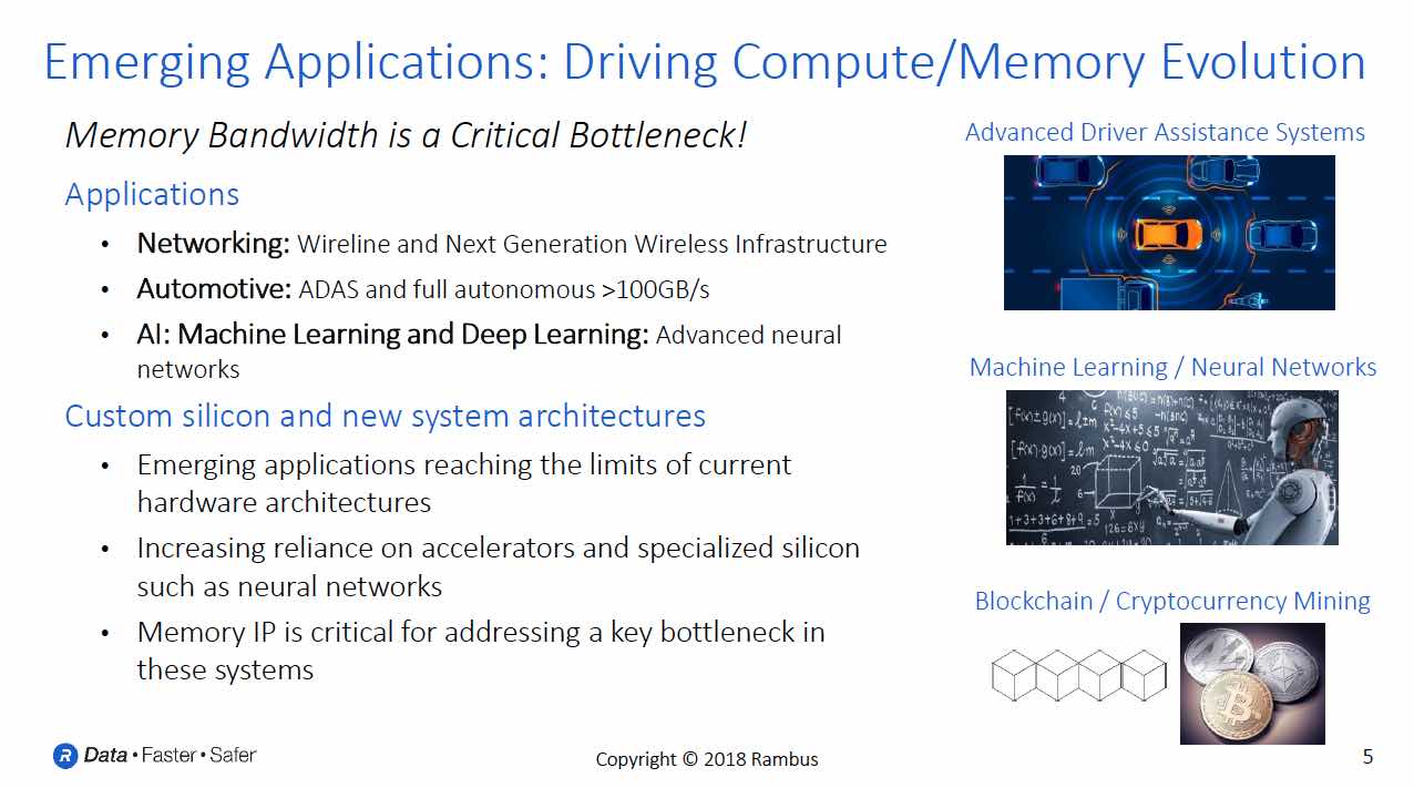
Let’s dive into the forces driving leading edge system design. According to Frank, with the exponential explosion of data creation, data centers are being pushed harder than ever to keep up with processing needs. Also, AI and automotive are other big factors that Rambus is seeing changing the requirements for systems. Traditional process scaling is slowing down and cannot be depended on to deliver performance improvements. Architectural changes are needed. One such example that came up in my discussion with Frank was how moving processing closer to the edge to aggregate and reduce the volume of data is helping. It is estimated that ADAS applications will demand 512 GB/s to 1000 GB/s to support Level 3 and 4 autonomous driving.
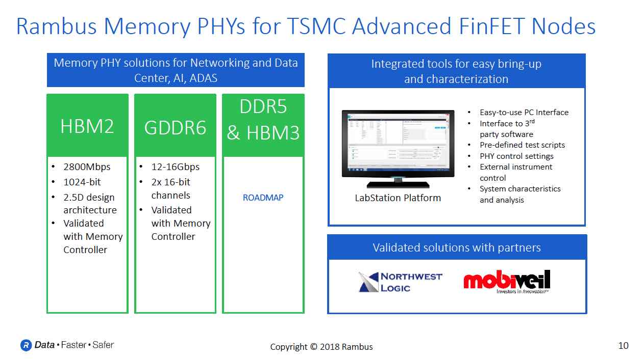
One of the major thrusts of his TSMC OIP talk is that GDDR is in a goldilocks zone for meeting these new needs. It is proven cost effective technology and has very good bandwidth – which is especially important for the kinds of parallel processing needed by AI applications. It also has good power efficiency. He cited the performance of the Rambus GDDR6 PHY, which has 64GB/s in bandwidth at pin rates of 16Gb/s. Their PHY supports 2 independent channels and presents a DFI style interface to the memory controller.

With their long experience in high speed interface design, Rambus is able to offer unique tools to their customers to help determine the optimal memory configurations for their designs. The Rambus tools also can help with design, bring up and validation of interface IP, such as the GDDR6 PHY.
Frank mentioned that they have an e-book available online that talks about GDDR how it is evolving to meet the needs of Autonomous vehicles and data centers. It has some great background information on these applications and also offer insights into how GDDR is advancing with in performance in 2018 with GDDR6. The e-book is available for download on their site.
Share this post via:


Why Your LLM-Generated Testbench Compiles But Doesn’t Verify: The Verification Gap Problem