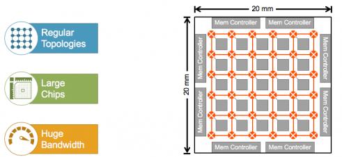
I wrote a while back about some of the more exotic architectures for machine learning (ML), especially for neural net (NN) training in the data center but also in some edge applications. In less hairy applications, we’re used to seeing CPU-based NNs at the low end, GPUs most commonly (and most widely known) in data centers as the workhorse for training, and for the early incarnations of some mobile apps (mobile AR/MR for example), FPGAs in applications where architecture/performance becomes more important but power isn’t super-constrained, DSPs in applications pushing performance per watt harder and custom designs such as the Google TPU pushing even harder.

At the high end, there is no pre-agreed set of “best” architectures. Everyone is experimenting to find the best performance per watt for their application. This is tricky. There are some needs in common with conventional computing – you want to quickly read in data, process computations, access and store to memory. However, maximally exploiting the spatially distributed nature of NN algorithms for performance and power pushes architects to distributed compute, most commonly in grids, rings or tori. These also exploit memory hierarchies, also distributed, and high-bandwidth memory (HBM) for bulk memory off-chip (or off-die in 2.5/3D packaging).
These architectures naturally push chip size, in the example above to 400mm[SUP]2[/SUP] and larger sizes are not uncommon. So now you have a hard problem in getting to timing closure across that big die. And if that wasn’t enough, ML typically requires massive amounts of data to be broadcast for image map and weight updates. So bandwidth demand in these systems can be huge, creating potentially massive traffic congestion and power problems.
Arteris IP has been working for many years with customers using ML technology, supporting near real-time inferencing at the edge with the likes of Mobileye, NXP, HiSilicon and others. But now they’re finding multiple companies wanting to support training at the edge, one very active direction for them coming from camera makers. And they’re seeing more activity around ML training acceleration in the datacenters. Of customers Arteris IP has announced, Baidu seems like an obvious fit here. Which in itself is interesting. After all, don’t NVIDIA dominate this space? Again, everyone’s looking for differentiation, not something you’re going to find if you’re just using the same platform everyone else is using. Not that Tegra isn’t a great solution but if you want to be at the bleeding edge, adding your own secret hardware sauce to your ML pipeline can be a way to pull ahead.

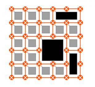
So what does all of this take? First, if you have distributed compute, you’re going to need an on-chip network to connect all of those compute nodes and the on-chip memory hierarchy and the off-chip memory. But it’s not quite as push-button as generating the grid in the opening graphic. In a strong NoC solution maybe you can dial in rings and tori, but these architects need more. Performance (and power) depends on very tightly coupled memory, so they want to embed local caches in the configuration. But there’s no fixed formula for where; they want to experiment to understand latencies and PPA implications. Those architects want to be to interact with network generation, to control where they want holes in the grid for memory blocks.

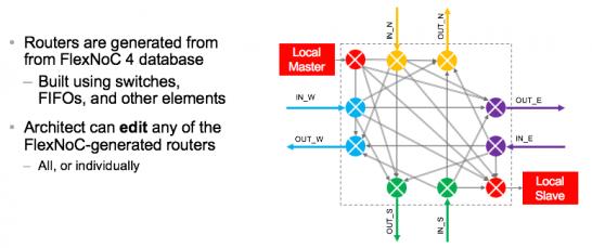
This goes further. High-end ML architects even want to tune the routers in the network they build, for example to add pipeline stages or FIFOs, or change the number of masters or slaves for a router or just one of the corner routers. All of these needs have implications for the architecture of the NoC generator. The standard method is compiler-centric. You dial in a bunch of parameters, interact through an interface to control details and generate. Which works very well in the processor and IP centered world for which this flow has been optimized over many years. But ML architects don’t have a standard recipe. They want to fool with almost everything, but they still want the benefit of automated generation, with all the flexibility of being able to customize the topology and the routers through that interface.
This is the first of 3 advances offered in Arteris IP’s just-announced AI package, available as an option to their recent FlexNoC4 release. They told me they have been working on this (and other features I mention below) for multiple years with their ML-driven customers. Kurt Shuler (VP Marketing) tells me these they’ve been responding to their customer ML needs, polishing and productizing this stuff for quite a while.
So, flexible network architecture (both logical and physical) while preserving the benefits of automating generation? Check. What about the big-die/timing closure problem? In general, timing closure across huge die isn’t a new problem. It’s very difficult to balance a clock tree across the full span of the design, so the standard solution is to use some kind of globally asynchronous, locally synchronous design technique. A popular solution is source-synchronous clocking; you forward the clock along with the data between locally synchronous domains. FlexNoC 4 includes support for a very lightweight approach that achieves this goal while minimizing congestion. The technology also provides support for multiplexing wires over long distances (again to mitigate congestion) using something they call VC-Links. Incidentally this solution is integrated with the Arteris IP PIANO timing closure package, so an architect can see where obstructions are and add virtual channels as needed.
Finally, there’s the bandwidth problem. One aspect is broadcast; how do you distribute lots of data to many destinations without dragging the whole system down? Through intelligent distribution is the Arteris IP answer. Distribute to a limited number of broadcast stations close to the destinations, then have those stations distribute locally. Obvious when you see it, but this requires a solution that supports architecting those broadcast stations into the network.
For traffic jams at HBM, the package provides methods to maintain high utilization of all connections into the memory controller through interleaving between initiators and targets, reorder buffers, traffic aggregation and data width conversions and support for very wide (1024 bits) connections where needed. Arteris IP have also added optimizations for datapaths, supporting up to 2048 bits wide.
All of which reinforces that design for AI/ML is not the same as design for traditional SoC components. The challenges are different and they require significantly enhanced solutions. You can learn more about FlexNoC 4 and the AI package HERE.
Share this post via:


Comments
3 Replies to “On-Chip Networks at the Bleeding Edge of ML”
You must register or log in to view/post comments.