I wrote earlier about managing service-level risk in SoC design, since the minimum service level a system can guarantee under realistic traffic is critical to OEM guarantees of dependable system performance. An ABS design which might get bogged down in traffic under only 0.1% of scenarios is of no use to anyone. That said, meeting target PPA goals remains a core benchmark for successful designs. PPA is still, presuming an architectural design and IP which should be able to meet those goals, a primary source of risk for high-complexity SoC designs in advanced processes.
The reason is simple to understand. Advanced designs depend on advanced architectures with high levels of parallelism connecting many cores through a very complex web of communication interconnect. That interconnect contributes 12% or more of the area to the design, it contributes important power consumption over and above contributions from the cores and, since it spans across what are typically very large chips, efficient design is critical to performance. PPA goals are dependent on system design, functional design and physical floorplan, and they can’t be guaranteed securely without balancing all three together.

It all hinges on a floorplan
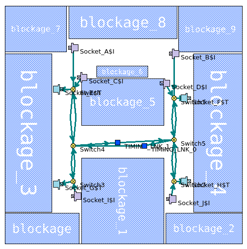
It’s difficult to consider floorplan constraints without a floorplan. Fortunately, some sense of how major functions should layout in the design should be available as early as product planning, even if it is only a hand sketch. Blocks from that sketch can be placed as physical constraints to guide a NoC design planning tool.

This will allow you to evaluate topologies (a tree in the example above), NoC component placement, and resource utilization within the available area. By visualizing the NoC design within the floorplan, you can identify areas of underutilization or excessive resource allocation. This insight helps in optimizing area utilization, reducing unnecessary resource duplication, and improving overall area efficiency.
Planning in this view also allows for approximate delay estimation through routes, in turn enabling you to plan latency minimization along latency critical paths or to add pipelining in paths that can handle increased latency. At the same time, you can weigh tradeoffs between bandwidth and network link widths. A wide link will support higher bandwidth but may increase congestion in that area, which should be readily apparent in an elaborated view of the plan.
Other options you might also consider to minimize area/congestion are compression/decompression (handled at initiators/targets) and traffic multiplexing through long-routes. You still provide mechanisms for these methods; the floorplan view helps highlight the need to make those choices as you are architecting the NoC.
Later in the design schedule, when a more complete floorplan is available, these options can be fine-tuned to optimize to that floorplan. Given the early optimization defined above, this really will be fine-tuning rather than a NoC rip-up and redesign that might be possible if the first design proves insufficiently flexible to adapt to the floorplan.
A very nice advantage of NoC architectures over crossbar structures is that they can be internally controlled for dynamic and static power, just as you can control other logic in the design. Clock gating is an option of course, but in the context of this topic, it is also worth considering power gating and voltage scaling options (commonly late-stage optimizations in this case). Taking advantage of these options depends on access to power/voltage domains, necessarily localized in the floorplan. You should have information about domain support for function blocks (CPUs, GPUs, etc.), suggesting possibilities for domain support in nearby NoC elements.
Design out PPA risk or hope for the best?
Interconnect design in complex SoCs built in advanced processes can be a significant contributor to PPA risk and, therefore, to missing target specs or design schedules. This risk is very much a factor of the close coupling between architecture, microarchitecture and implementation in today’s advanced designs.
That risk is very manageable when considering interconnect design within the context of the SoC floorplan, estimated initially and later refined. Check out Arteris IP’s FlexNoC 5 to get more details on how you can remove risk from your SoC designs.
Share this post via:


Comments
There are no comments yet.
You must register or log in to view/post comments.