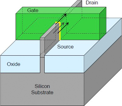
 We have all heard that planar transistors have run out of steam. There are two ways forward. The one that has garnered all the attention is Intel’s trigate which is their name for FinFET. The other is using thin film SoI which ST is doing. TSMC and Global seem to be going the FinFET way too, although at a more leisurely pace. But why are planar transistors running out of steam? And why are these the two promising ways forward? Dr Chenmin Hu, the inventor of the FinFET first described in a 1999 paper (pdf), gave us all a tutorial. It was fascinating. I thought that most of the power of the FinFET came because the gate wraps around the channel on three sides and three is better than one. But that is not the real story.
A planar MOS transistor theoretically should have a performance of 63mV/decade (which comes from the distribution of electron potentials trying to get out of the source through the gate). But this assumes that all of the channel region is fully controlled by the gate. The deeper down into the channel you go, and thus the farther from the gate, the less it is controlled. In practice, this means that current can slink through even when the gate is “off” which is why leakage power has become such a big problem. In effect the transistor has become a resistor and cannot control the current.
 Solution #1: reduce the oxide thickness. This is what we have done for decades. But this still cannot control the channel far from the gate since the voltages have come down too. So the solution is to ensure that there is no silicon far from the gate. That way the whole channel will be well-controlled by the gate.
There are two ways to ensure that there is no silicon far from the gate. One is the FinFET. Build a fin (the name comes from being like a fin on a fish) for the channel and then wrap the gate over the top of the fin. The key parameter is to make the fin thinner than the gate width. That way the whole channel is completely controlled by the gate since everywhere in the channel is close enough to the gate. Working FinFETs have been built at 5nm and 3nm (using e-beam so not economic for mass production, but the technology works at those dimensions).
There have been two big improvements to the FinFET since the original paper in 1999. Firstly TSMC worked out how to put thin oxide on top of the fin (the original fin was effectively 2-sided). Intel is the company first making use of this but, as Dr Hu pointed out, TSMC can take credit. Ironic. The second is in 2003 Samsung worked out how to build FinFETs on bulk substrate (they were SoI in the original paper).
Since FinFET and planar transistors use many of the same manufacturing steps and are completely compatible, the low risk approach would be to mix them and have both available on the same chip. So apparently it was a surprise when Intel decided not to do this and have a FinFET-only process at 22nm.
The second way to make sure that there is no silicon far from the gate is to go away from a bulk silicon process and instead use an insulator, put a thin layer of silicon on it, and then build planar transistors in the normal way. There is no silicon far from the gate because if you go that deep it is no longer silicon, you are into the insulator layer (where obviously no current can flow).
 This is the approach ST is taking and was explained in a lot more detail by Joël Hartman of ST. They believe that it has the best speed/power performance. The gate region is fully depleted so this technology is known as FD-SOI (not quite as catchy as FinFET or even Tri-gate). ST reckon that due to lithographic reasons 28nm will be a golden-node with a long lifetime. They currently have planar 28nm and they are introducing FD-SOI first at 28nm as a sort of second generation, before introducing it at 20nm. They also feel that without some unanticipated breakthrough neither EUV nor double/triple patterning will be economical at 14nm and they will probably have a process in the gap that for now they are calling 16nm although it might be anwyhere between 14 and 20nm (with a less complex process).
So there you are: planar transistors are at the end of their life because too much silicon is far from the gate and so not turned off by the gate. So make sure no silicon is far from gate. Either build a thin fin and wrap the gate around it, or switch from bulk silicon to a thin film of silicon on an insulator. Hence the future is FinFET and/or FD-SOI and we’ll see how this plays out.
Share this post via:


Silicon Insurance: Why eFPGA is Cheaper Than a Respin — and Why It Matters in the Intel 18A Era