
IC device physics uncovers limits to reliable operation, so IC designers are learning to first identify and then fix reliability issues prior to tape-out. Here’ s a list of reliability issues to keep you awake at night:
- Time Dependent Dielectric Breakdown (TDDB)
- Negative Bias Temperature Instability (NBTI)
- Hot Carrier Injection (HCI)
- Threshold Voltage Shift (Vt)
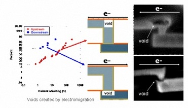
- Electromigration (EM)
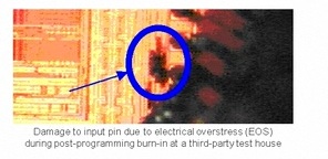
- Electrical Overstress (EOS)
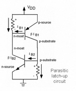
- Latch-Up
- Electro Static Discharge (ESD)

Reliability Analysis
The traditional approach to reliability analysis has been simulation which can take a long time to run, and the results are only as good as your extracted SPICE netlist, SPICE models, stress models, and input stimulus.
Another approach is to use traditional DRC rules to find reliability conditions which requires adding extra layers, or “marker layers” to the IC layout database. Adding marker layers is still a manual process and is ripe for mistakes, plus it adds additional DRC runs costing you more time.
The oldest approach is to eyeball your IC layout and come to a conclusion about what structures may be causing you a reliability problem, then go back and tweak the layout again. There’s not much science or repeatability involved with this approach.
An Emerging Reliability Analysis Approach from Mentor Graphics
Back in 2008 I first learned about a new EDA tool from Mentor Graphics called Calibre PERC (Programmable Electrical Rule Checker), that was initially aimed at ESD designers to help pinpoint and fix their IC layout that was susceptible to ESD failures. Today I had an update meeting with Matthew Hogan at Mentor Graphics in Wilsonville, Oregon to understand what has been happening with Calibre PERC as it applies to reliability analysis.

PERC now has access to the schematic netlist, IC layout, current density, foundry reliability models, and voltages propagated to any node in the netlist. Some of the reliability checks that PERC can automate for you include:
- Topology and layout-based checks
- Signals crossing multiple power domains (level shifters, diodes)
- EOS
- Current density (CD)
- Point to point (P2P) resistance
- Hot gate, diffusion identification
- Layer extension
- Device matching
- Decoupling Capacitor placement
- Forward biased PN junctions
- Power domain checking (presence of level-shifters, type of level-shifter)
- Data retention cell checking
- Thin-oxide gates connected with proper bulk
- Identify EOS without circuit simulation using Voltage Propagation and static techniques
- Detect over-voltage conditions
- Find device breakdown and reverse current issues in high voltage areas
- Pinpoint electrical floating gates and floating nodes
- Voltage mismatches at domain interfaces
- Maximum voltage across gate oxides
- Voltage dependent DRC checking
- Spacing checks based on Vdd levels without using marker layers
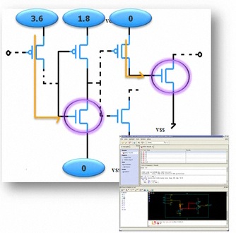
The Voltage Propagation feature is something new with PERC since I last chatted with Mentor folks and it offers a way to measure voltages at any node in your design without having to run SPICE circuit simulation. These node voltages are then used to check if all the voltage and spacing rules are being properly followed.
The closest EDA tool to PERC that comes to mind was something that we used at Intel called the Coarse Leve Circuit Debugger (CLCD), back in the 80’s.
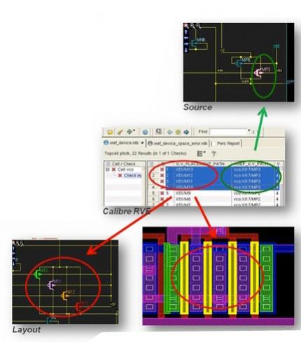
How does PERC work?
[LIST=1]
Who is Using Calibre PERC?
The good news is that the PERC approach is also supported by leading foundries like TSMC in both their AMS and Digital Reference Flows, plus you can even add your own programmable rules specific to your industry requirements. Big companies like VIA Technology and Fujitsu are using Calibre PERC to improve their IC reliability, along with smaller companies like Skyworks. TSMC gave the Calibre PERC team the Customer Choice Award in December 2011 as part of their Open Innovation Platform meeting.
Conclusions
Mentor is well-known for the Calibre product line used in DRC and LVS, and now PERC is adding new features to make your IC design more reliable without having to run as much circuit simulation or manually add marker layers to the layout. The first industries adopting PERC include automotive and medical.
I suspect that Cadence and Synopsys will have to play catch-up in this product area because they don’t really offer anything comparable to Calibre PERC, just DRC and LVS tools.
To preview the full presentation and product demo visit www.calibreperc.com, and they will send you an email link to, “Calibre PERC: Effective Reliability and Low Power Verification”.


Comments
9 Replies to “IC Reliability and Prevention During Design with EDA Tools”
You must register or log in to view/post comments.