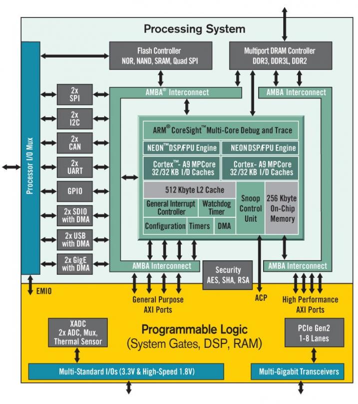


Just as important as block RAMs, IO and DSP48’s is what interconnect or fabric is going to be used when considering SoC FPGA designs. I think Xilinx has found the winning combination. What is paramount to the new SoC FPGA methodologies is not only the challenge of moving huge amounts of data around; we are now to consider data movement to/from ARM processors and its external memories like within the Xilinx Zynq series FPGAs.
Traditionally FPGA architects really do not want to use standard interfaces within the internal FPGA design. They just register or buffer data and move it to the next processing block in the design. But SoC designs, for the sake of design time, simplicity, integration and reuse will require a standard bus interface. Xilinx has chosen what I believe is a stellar path for bridging the data path gap of external memories like DDR, Programmable Logic within the FPGA and ARM processors. Advanced eXtensible Interface (AXI) Interconnect comes to the rescue. We simply just cannot hack together or write spaghetti code no longer. Did I say we? I meant me.

A great example of the AXI bus in use is in the Xilinx white paper XAPP792 “Designing High-Performance Video Systems with the Zynq-7000 All Programmable SoC”. By all means give this paper a read and you will see as in many of the Xilinx white papers they have done much work for the designer already, including very fine reference designs. AXI is very flexible in which Xilinx has an AXI lite variant which is easy on the resource usage and the streaming AXI core which is perfect for high speed real time applications such as streaming video and even RADAR. Since you are designing modules with AXI interfaces, reusable libraries can be developed. The crossbar functionality is where the AXI bus is the winner, think of it as a backplane fabric within a chip and it points to the future of silicon system interoperability ; Network On a Chip (NoC) , that is moving data to anywhere without a huge latency penalty.
Looking into XPP792, Xilinx has designed an ARM+PL (programmable logic)+AXI video framework (for free). We often take for granted what can be done in FPGAs and the mass amounts of free knowledge out there. Think back how long this video application would have taken to design back in the Virtex4/5 days. Probably many months for the seasoned FPGA designer. As FPGAs increase in density and SoC is the reality, standard interfaces are no longer an option but a must, and once again Xilinx has picked a winner with its partnership with ARM and it’s AXI bus.

lang: en_US


TSMC CoWoS versus Intel EMIB Semiconductor Packaging