Array
(
    [content] => 
    [params] => Array
        (
            [0] => /forum/index.php?threads/questions-regarding-semiconductor-manufacturing.19924/
        )

    [addOns] => Array
        (
            [DL6/MLTP] => 13
            [Hampel/TimeZoneDebug] => 1000070
            [SV/ChangePostDate] => 2010200
            [SemiWiki/Newsletter] => 1000010
            [SemiWiki/WPMenu] => 1000010
            [SemiWiki/XPressExtend] => 1000010
            [ThemeHouse/XLink] => 1000970
            [ThemeHouse/XPress] => 1010570
            [XF] => 2021370
            [XFI] => 1050270
        )

    [wordpress] => /var/www/html
)

Questions regarding semiconductor manufacturing

Hello folks,

I am currently diving deeper into the front-end of semiconductor processing and checking multiple sources to learn how it works. I came across multiple videos on YouTube and want to check with you guys if my understanding is correct. I attach a small PDF presentation that I quickly made that goes through all the process steps, on how to get a transistor onto a bare wafer. Could you please check if the process flow and therefore my understanding is correct?

Am I understanding it correctly, that a "deposition process" is basically process step 8) and 14) from my PDF? In step 8, how does the "gaps" of the oxide layer get filled up?

Is step number 7 from my PDF what people refer to as doping? Is this the only time doping is necessary? How is this done? Is this basically "liquid n-doped Silicon" that is put there? And how is it put there?

I saw on YT a video from Samsung, explaining the process:
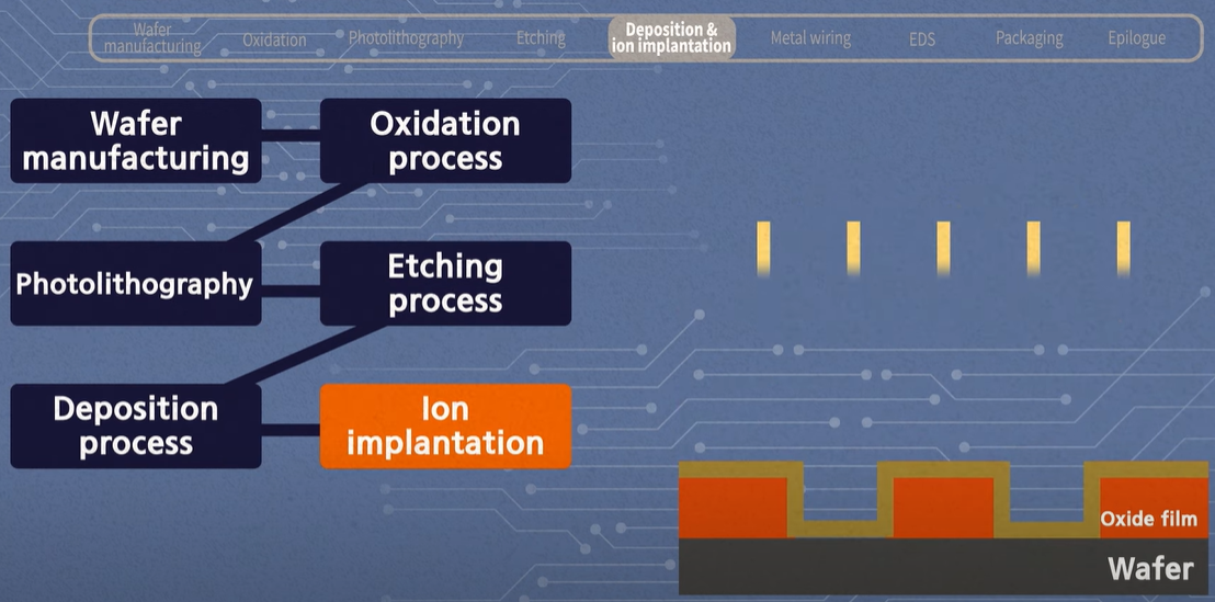
1711633992579.png


In this picture, they show that the ion implantation comes after the deposition process? Isn`t this wrong? In this case the n-doped area of Silicon would be above the metal layer? This makes no sense to me? Besides this, in the schematics bottom right, there do not show the p- and n-type area in the wafer.

I hope someone can help me understanding this.

Thanks,
Tobias
 

Attachments

  • Transistor Making.pdf
    311.6 KB · Views: 40
Because transistors are three dimensional objects that need to be constructed and then etched out to provide channels through out.
 
I also found another video from Infineon:


The final result is obviously the same but am I correct in my thinking, that this is a different process flow in terms of what process comes when compared to my PDF file?
 
Hello folks,

I am currently diving deeper into the front-end of semiconductor processing and checking multiple sources to learn how it works. I came across multiple videos on YouTube and want to check with you guys if my understanding is correct. I attach a small PDF presentation that I quickly made that goes through all the process steps, on how to get a transistor onto a bare wafer. Could you please check if the process flow and therefore my understanding is correct?

Am I understanding it correctly, that a "deposition process" is basically process step 8) and 14) from my PDF? In step 8, how does the "gaps" of the oxide layer get filled up?

Is step number 7 from my PDF what people refer to as doping? Is this the only time doping is necessary? How is this done? Is this basically "liquid n-doped Silicon" that is put there? And how is it put there?

I saw on YT a video from Samsung, explaining the process:

View attachment 1796

In this picture, they show that the ion implantation comes after the deposition process? Isn`t this wrong? In this case the n-doped area of Silicon would be above the metal layer? This makes no sense to me? Besides this, in the schematics bottom right, there do not show the p- and n-type area in the wafer.

I hope someone can help me understanding this.

Thanks,
Tobias
Hi, I see a major problem in your pdf: in step 7, n-doped silicon cannot magically appear in the voids of step 6 (certainly not as a consequence of PR removal). As a matter of fact, in step 6 there is no reason to etch away that bit of silicon below the oxide. Doping (typically performed by ion implantation) does not add silicon to the wafer, it puts dopant atoms INSIDE the silicon that's already there. Basically you launch high-energy atoms towards the exposed silicon, they enter the silicon, lose kinetic energy and finally stop a few nm (or even hundreds on nm, depending on the energy) inside the silicon. When you do an ion implantation, you protect the silicon (with PR or oxide or whatever) where you DON'T want doping.
 
Hi, I see a major problem in your pdf: in step 7, n-doped silicon cannot magically appear in the voids of step 6 (certainly not as a consequence of PR removal). As a matter of fact, in step 6 there is no reason to etch away that bit of silicon below the oxide. Doping (typically performed by ion implantation) does not add silicon to the wafer, it puts dopant atoms INSIDE the silicon that's already there. Basically you launch high-energy atoms towards the exposed silicon, they enter the silicon, lose kinetic energy and finally stop a few nm (or even hundreds on nm, depending on the energy) inside the silicon. When you do an ion implantation, you protect the silicon (with PR or oxide or whatever) where you DON'T want doping.
Ok, understood. So the etching does not remove the Silicon but only the oxide layer above.

The n doping in this specific area (which at the end is the drain and source area) come from ion implantation.

In the infiniin video I posted they were talking about polysilicon......Is this the material they use for the "metallization"?
Polysilicon is just short for POLYcristalline SILICON. Highly doped polysilicon was once used instead of metal for the gate electrode. There are (were) a few good reasons for this, but you should probably refer to a solid reference book instead on multiple YT videos if you want to understand a full CMOS fabrication sequence. There is a dated but excellent book at https://plummergriffinbook.stanford.edu/previous_book and can be downloaded for free. Chapter 2 gives a detailed sequence of an old (late nineties) technology, but many points are still relevant today.
 
Polysilicon is just short for POLYcristalline SILICON. Highly doped polysilicon was once used instead of metal for the gate electrode. There are (were) a few good reasons for this, but you should probably refer to a solid reference book instead on multiple YT videos if you want to understand a full CMOS fabrication sequence. There is a dated but excellent book at https://plummergriffinbook.stanford.edu/previous_book and can be downloaded for free. Chapter 2 gives a detailed sequence of an old (late nineties) technology, but many points are still relevant today.
Hello Francesco,

thanks for the book, really interesting, I am currently going through it and already a couple of questions popped up:

Chapter 2.2.2 Active region formation

When I understood it correctly, the book describes two different approaches to forming the different regions on the wafer, where the active area will be placed afterwards:

Either LOCOS or STI. The final result, even though with maybe slightly different geometrical forms of the layers and barriers, is of course the same.

Question 1:

Si3N4 layer on top of SiO2. Why is the Si3N4 layer necessary. For one, it is used to compensate for the induced stress of the SiO2 but also necessary in the next step, baking the wafer in an oxidizing ambient, it impeds the SiO2 to grow in the area covered by Si3N4, correct? Is there any other necessity for the Si3N4 or is this the only one?

In general, is this still used today since the book is alreay a bit older? Or is it done differently nowadays?

Regards.
Tobias
 
STI is still done today, LOCOS on the other hand is obsolete. You are right about the purpose of the nitrite, it constrains the STI oxide to grow into a nice isolation structure. As for other uses I can think off of the top of my head, SiN caps over the NMOS gate are used to provide tensile strain to the channel and increase NMOS carrier mobility. Another use for nitride films is they are really nice tools for making selective etches. A super common trick is tuning an etch chemistry to be selective to nitrides or oxides and using the other material to protect whatever is underneath from being etched.
 
Back
Top