Designing at the 20nm node is harder than at 28nm, mostly because of the lithography and process variability challenges that in turn require changes to EDA tools and mask making. The attraction of 20nm design is realizing SoCs with 20 billion transistors. Saleem Haider from Synopsys spoke with me last week to review how Synopsys has re-tooled their EDA software to enable 20nm design.

Saleem Haider, Synopsys
20nm Geometries with 193nm Wavelength
Using immersion lithography the clever process development engineers have figured out how to resolve 20nm geometries using 193nm wavelength light, however to make these geometries yield now requires two separate masks, called Double Patterning Technology (DPT).
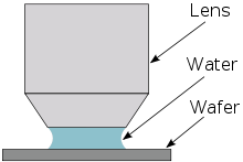
Immersion Lithography, source: Wikipedia
With DPT you have to split a single layer like Poly or Metal 1 onto two separate masks, then the exposures from the two masks are overlaid to produce that layer with 20nm geometries.
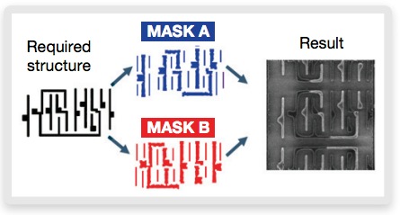
Double Patterning Technology (DPT)
Looking ahead to 14nm and smaller nodes this trend will continue with three or more patterns per layer.
When a mask layer is turned into two parts the process is called coloring, and the trick is to make sure that two adjacent geometries are on different colors.
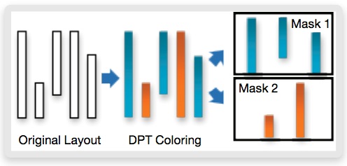
DPT Coloring
With DPT you have to make sure that your cell library and Place & Route tool are both DPT-compliant.
Often in your IC layout the DPT process will have to use stitching to accomodate via arrays:
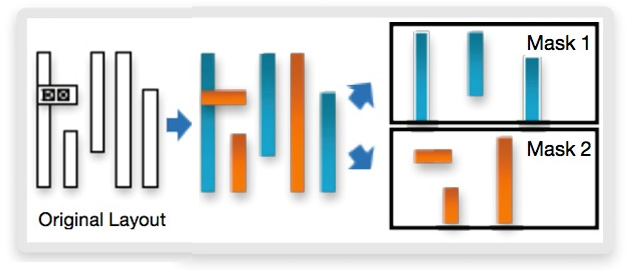
This stitching will cause issues with line-end effects that in turn can degrade yield:
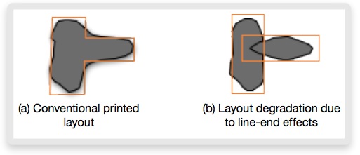
The earlier that you identify these issues, the sooner that you can make engineering trade-offs.
Foundries create layout rules at 20nm to specify how to produce high yield, and there are some 5,000 rules at this node.
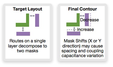
Using DPT techniques will also cause a variation in capacitance values between adjacent nets caused by subtle shifts in the double masks.
DPT-Ready EDA Tools
Synopsys has updated their EDA tools to enable 20nm design, specifically:
- Logic synthesis, Design Compiler
- Place and Route, IC Compiler
- DRC and LVS, IC Validator
- Parasitic Extraction, StarRC
- Static Timing Analysis, Primetime
- Circuit Simulation, HSPICE
- Custom IC Layout editing, Custom Designer
Q&A
Q: Where can I read more about 20nm design with Synopsys tools?
A: Achronix did a paper at the Synopsys User Group, and they fabricated at Intel’s custom foundry using FinFET technology.
Q: How popular is your DRC and LVS tool, IC Validator?
A: There have been 100 tapeouts in the past year for IC Validator tool.
Q: How many 20nm designs are there?
A: Test chips were done first last year, and now production designs are taping out with commercial foundries.
Q: How many mask layers require DPT in a 20nm design?
A: It depends on the foundry. First layer metal, maybe second layer of metal. As you relax the metal pitch, then you don’t need DPT. Poly needs DPT.
Q: What about mask costs at 20nm with DPT?
A: It adds to the costs. It’s always a trade off, the foundry can relax the pitches and void DPT usage.
Q: Which foundries have qualified 20nm with Synopsys tools?
A: TSMC, Samsung, GLOBALFOUNDRIES have qualified and endorse the Synopsys flow for 20nm.
Q: What can you tell me about your Custom IC design tools?
A: Our custom tools are also DPT aware, (SpringSoft, CiraNova, Custom Designer) – coming together.
Q: Why should I visit Synopsys at DAC?
A: We’ll have live product demos, talk about advanced nodes, show emerging nodes, 14nm, 16nm, discuss new product features, and have special events. There is an IC Compiler luncheon where customers speak, and that’s on Monday.
Further Reading
- White Paper: Design Solutions for 20nm and Beyond


Comments
0 Replies to “Challenges of 20nm IC Design”
You must register or log in to view/post comments.