Intel is the number one semiconductor company in the world and has taken the lead in bringing FinFET (aka Tri-Gate) silicon to market at the 22nm node starting in May 2011, so now we see the pure play foundries playing catch-up and start talking about their own FinFET roadmaps. IC designers and layout engineers want to know how their design methodology will change as they consider using a FinFET process compared to a planar process.
Jamil Kawaat Synopsys has just written a new White Paper, Designing with FinFETs: The Opportunities and the Challenges. This blog summarizes the major points of the White Paper on FinFETs and how it effects the IC design process.
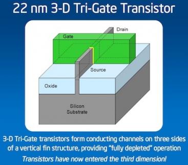
Source: Intel
There’s a bit of marketing hype in the Intel statement of transistors now entering the third dimension because all planar transistors have three dimensions, it’s just that the FinFET is notably taller than planar CMOS transistors.
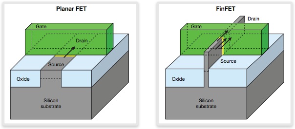
Simplified transistor comparison not drawn to scale, Planar vs FinFET
Attractive features of the FinFET transistors include:
- Lower leakage currents caused by a fully depleted channel region
- Reduced short-channel effects
- More transistors/unit area due to 3D layout
- Less variation effects from dopant fluctuation
- Lower Line Edge Roughness (LER) variation
- Improved performance margins
- Lower retention voltage in SRAMs
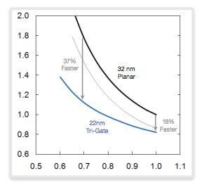
Intel’s 22nm Tri-Gate technology showing a wider performance advantage at lower VDD
Source: Mark Bohr, Intel. May 2011.
Negative consequences of using FinFET devices are:
- Quantized channel widths, fewer choices compared to planar CMOS
- More complex SPICE models, longer simulation run times
- More complex extraction rules and longer extraction run times
- Body-biasing techniques lose their effectiveness
- Additional Restricted Design Rules (RDR)
- New Layout Proximity Effects (LPE)
- Reliability concerns, Negative-Bias Temperature Instability (NBTI) and Positive-Bias Temperature Instability (PBTI)
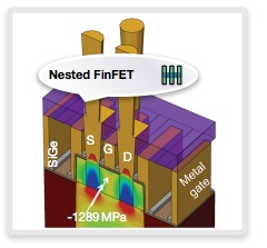
Stress simulation of FinFETs
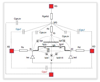
Parasitics model of the FinFET
With the increased number of layout rules for FinFET devices you want to use a rule-driven layout flow, instead of the old sequential flow of: Schematic design, Layout design, batch rule check, iterate until correct.
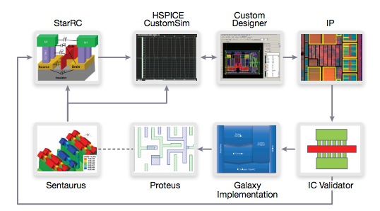
EDA Tool Flow
Synopsys has seven EDA tools used to implement FinFET-based IC designs:
[TABLE] style=”width: 500px”
|-
| EDA Category
| EDA Tool
|-
| TCAD modeling
| Sentaurus
|-
| Parasitic extraction
| StarRC
|-
| SPICE circuit simulation
| HSPICE, CustomSim
|-
| IC schematic and layout editing
| Custom Designer
|-
| DRC and LVS checking
| IC Validator
|-
| Implementation (Logic Synthesis, P&R)
| Galaxy
|-
| Mask synthesis
| Proteus
|-
Summary
Intel started using FinFET devices at the 22nm node in 2011 while other foundries have announcements for FinFETs at 14nm nodes coming up in 2013 and later. EDA tool flows have been updated to account for the new FinFET issues, so the big question that remains is silicon pricing and yield compared to planar technology.
Read the complete White Paper here after a brief registration process.
Related Reading
- FinFET Wiki
- GLOBALFOUNDRIES Announces 14nm Process
- Intel’s finfets too complex and difficult?
- FinFET Standard Cells at DAC
- Industry Standard FinFET versus Intel Tri-Gate!
- Intel Tri-Gate is in Trouble?!
- Next Generation Transistors: a Tutorial from the Master
- Introduction to FinFET technology Part II
- Introduction to FinFET technology Part I


Comments
30 Replies to “Designing with FinFETs”
You must register or log in to view/post comments.