When I worked at EDA vendors and attended DAC, one of the most popular questions asked in the booth and suites was simply, “What’s new this year?” It’s a fair question, and yet many semiconductor professionals are so focused on their present project, using their familiar methodology, that they simply aren’t aware of all of the industry changes, and specifically EDA tool updates. I was made aware of several changes to the popular EDA tool family called Calibre RealTime and Calibre Recon from Siemens EDA, announced this week at DAC, so here’s my take on them.
What’s Changed
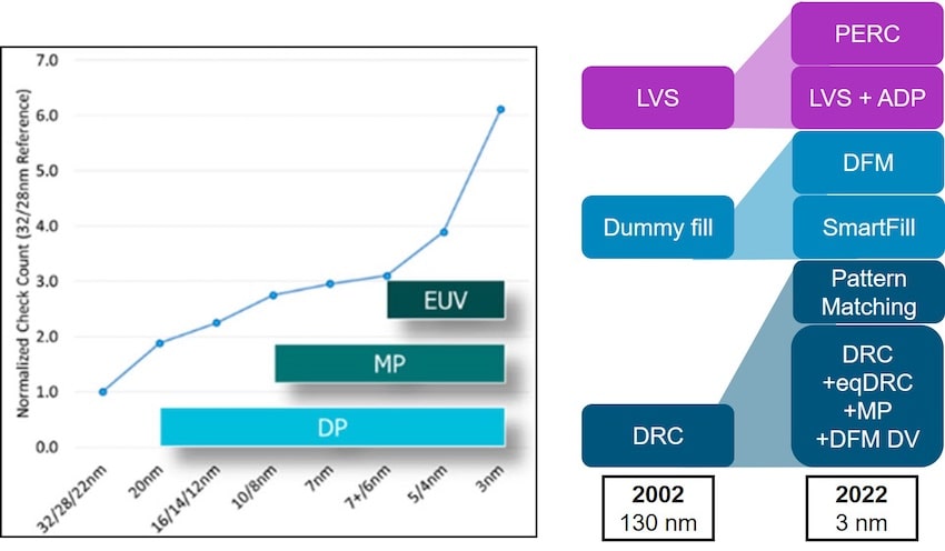
In the past two decades of semiconductor design we’ve moved beyond the simple EDA requirements of getting a cell, block and chip to be DRC clean, LVS clean and DFM ready with dummy fill. In leading-edge process nodes the types of analysis and number of foundry rules have just exploded, and IC masks started using Double Patterning (DP), Multi-Patterning (MP) and finally EUV.

Calibre RealTime Custom
The earliest Design Rule Check (DRC) and Layout Versus Schematic (LVS) tools were designed to be run in batch mode, so engineers submitted their jobs, went to lunch, then in the afternoon viewed the errors and communicated with the layout designers on what and where to fix each violation. Sounds too labor intensive and time consuming.
In recent years the new idea of running these DRC and LVS checks live, while the layout designer was working on the physical design came into vogue, bringing along a more efficient methodology, saving time by having near instant feedback, instead of waiting for a batch job to finish in a queue. The big question with a real time running of DRC has always been, “Are these checks approved by the foundry, and are they complete or just a reduced subset of the rule checks?”
The new productivity feature with Calibre RealTime Custom is that it now automatically tracks DRC across multiple regions, so that multiple edits can be fixed, tracked and checked simultaneously. This enables a team-approach to reaching DRC clean in real time possible, and the benefit is saving precious time. Oh, and the checks are signoff-quality too.
Calibre RealTime Digital
Design For Manufacturing (DFM) requires that the IC surface be more planar, instead of having hills and valleys, so adding dummy fill was a starting point for automating. Advanced nodes down to 3nm require more than dummy fill, and now Calibre RealTime Digital supports in-design fill by using the Calibre Yield Enhancer SmartFill, so designers enjoy a foundry signoff fill by using the design cockpit. It’s a faster way to be DFM ready.
Calibre nmDRC-Recon
Alex Tan blogged earlier about Calibre Recon here, and it’s a way to reduce the number of DRC checks and violations, in order to pinpoint the biggest layout issues first. The new feature with Calibre nmDRC-Recon when using Calibre RealTime Digital is that you can “gray-box” out some of your cells and blocks that are still works in progress, while still checking DRC for all the connections to adjacent blocks and even the upper-level metal layers. Fast feedback, earlier.
Calibre nmLVS-Recon
Finding a fixing interconnect shorts using Calibre LVS was blogged by Tom Dillinger earlier. What’s new with Calibre nmLVS-Recon is that you can run short isolation (SI) mode several times per day, instead of waiting overnight for results. Designers continue to use the same design inputs and foundry rule decks as before, so it’s simple to learn and get running with earlier results.
Summary
Calibre has quite a broad family of tools, where each one is optimized for a specific physical verification or reliability task. What started out as only a batch-oriented EDA tool, has now blossomed into interactive versions that provide earlier feedback and faster times to a clean IC design and layout. New features have been added and announced at DAC this year, so the automation benefits just keep growing to tackle all of the new process node complexity increases. The Calibre tools also work inside of your favorite IC layout, design and physical implementation tools, while providing a consistent UI experience, so go ahead and mix-and-match vendors.
If you attend DAC this year in San Francisco, then make your way over to the Siemens EDA booth, it’s #2521, located on the second floor. Ask the experts in the booth, “So, what’s new this year?”
Related Blogs
- Symmetry Requirements Becoming More Important and Challenging
- EDA in the Cloud – Now More Than Ever
- RealTime Digital DRC Can Save Time Close to Tapeout
- Mentor Cuts Circuit Verification Time with Unique Recon Technology
- Accelerate Your Early Design Recon
- A Fast Checking Methodology for Power/Ground Shorts


Comments
There are no comments yet.
You must register or log in to view/post comments.