Advanced board designs are fertile ground for misbehavior in time and frequency domains. Relying on intuition, then waiting until near-final product for power integrity (PI) or EMI testing almost guarantees board respins are coming. Lumped-parameter simulations of on-board power delivery networks (PDNs) struggle with predicting behavior in the face of parasitics. A new series of Keysight engineering webinars dive inside PDNs with critical insights on where PI problems develop. Results from Keysight’s board-level EM simulation and EMI compliance analysis tools and techniques can help teams reduce late respin drama.
Modeling on-board power delivery
One of these webinars tears into decoupling capacitors. If a few are good, more must be better, right? That myth gets busted quickly, and so does another. Capacitor manufacturers want engineers to think they’re buying a certain value of a capacitor. Instead, what every manufacturer ships is a bundle of impedance with resistance, inductance, and capacitance.
Now multiply by a bunch of decoupling caps of different values across a board. Clean power delivery and controlled EMI depend on how those capacitors interact with loads, and each other, at various frequencies. A PDN provides three sources of power:
- The voltage regulator module (VRM), which resembles a low-pass filter. At higher frequencies, the VRM control loop falls behind and its output impedance goes inductive.
- The decoupling capacitors, which become a bandpass filter as they also go inductive beyond their self-resonant frequency.
- Any on-chip capacitors and parasitic package capacitance, not large enough to supply power at lower frequencies but able to stabilize delivery as frequency increases.
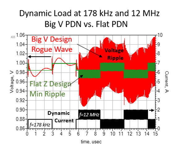
Minimizing voltage ripple and preventing the “rogue wave” resonance calls for flat impedance from those three sources over a range of frequencies.

The discussion continues with a look at the pitfalls of lumped-parameter EM simulations, then wraps up with an in-depth FPGA placement case study. “The simulations are only as good as the models,” says Keysight’s Heidi Barnes, SI/PI Application Engineer. Keysight helps vet and optimize capacitor models used in its PathWave ADS PIPro EM simulation tool – for example, models with capacitor package mounting inductance removed improve results. The EM field solver in PIPro generates an S-parameter model, including all components and parasitic effects, enabling board-level EM simulation matching real-world measurements.
Going back to the power source with board-level EM simulation
Another webinar in this series looks at one specific type of design: switched-mode power supplies (SMPS). Switching magnetics reduces size and improves efficiency but throws off noise and EMI as part of the process. Power supplies also fall under a wide range of EMI compliance specifications in different geographic markets and application segments. Designs again often fall victim to expensive late-stage test failures and respins, especially when moving from one market where testing passed to another market with a different profile.
Noise correlates to the high switching speeds and currents, or high di/dt in industry terms. Square-wave switching waveforms also throw off strong harmonics at even higher frequencies, up into RF ranges. Wide band gap (WBG) transistor technology, such as GaN or SiC, is also changing the picture. These technologies lower impedance and enable higher switching speeds. But, parasitic effects once buried by more dominant terms now rise to the surface.
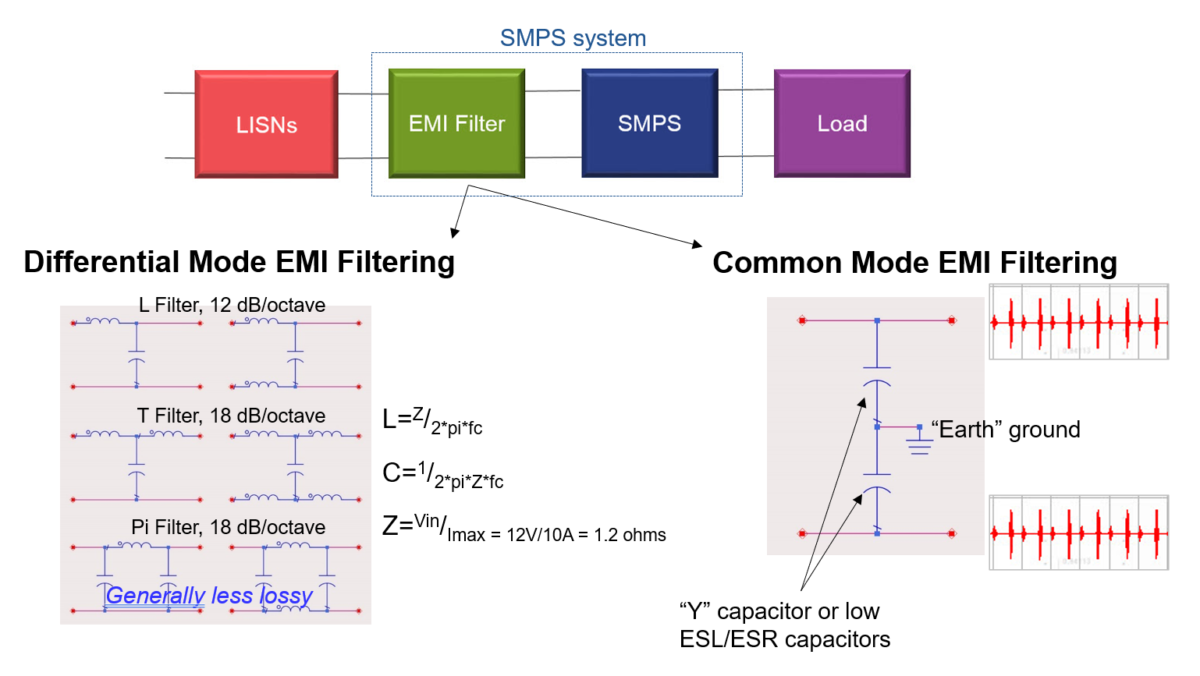
“The pre-layout schematic simulation using Spice gives you a best-case result,” according to Steven Lee, Product Manager for Keysight PathWave Power Electronics. That can trap SMPS engineers in a complex test-respin cycle where differential noise, common mode noise, resonance and harmonic spikes are hard to predict and mitigate. Adding EMI filters can have unexpected effects as capacitors and board parasitics reveal their impedance characteristics.

A more effective approach for better EMI results is post-layout simulation and layout adjustments, introducing minimal EMI filtering. Using Keysight PathWave ADS PEPro brings layout-based design and board-level EM simulation technology optimized for power electronics, with similar field solvers for parasitic extraction. Steven walks through a demo of PEPro during the webinar.
Analyzing EMI compliance quickly
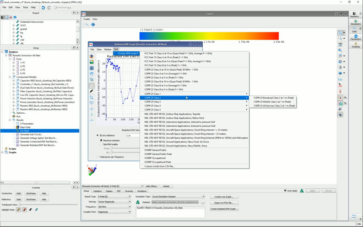
A big workflow improvement is the EMI compliance overlays in PEPro. Instead of manually scanning and comparing EMI plots to specifications, pre-loaded compliance profiles including FCC Class A and B, CISPR 22 Class A and B, and CISPR 25 Class 1 through 5 can drop over simulation results with a couple of clicks.

Tightening the loop between developing higher fidelity EM models, making board layout adjustments accounting for parasitics and impedance behavior over frequency, and visualizing EMI compliance virtually before moving to physical test are big breakthroughs.
“You should be board-level EM simulating”
The main takeaway from this Keysight webinar series is power integrity and power electronics teams should be simulating to know more about their designs sooner. If teams had prior experience simulating with less accurate models and lumped parameters, it’s time to bring in better board-level EM simulation tools that can help shift-left virtual testing, leaving the late respin drama behind.
Webinars available on-demand now:
Optimizing Capacitor Selection and Placement for Power Integrity
Reduce EMI in Switched-Mode Power Supply Design
Future live events:
Both Heidi and Steven have new, live webinars coming with more thoughts on PI and EMI in the coming months – watch the main Keysight Webinars page for these and other live events.
Also Read
Shift left gets a modulated signal makeover
Share this post via:


Comments
There are no comments yet.
You must register or log in to view/post comments.