Photonics IC’s (PIC’s) are used to transmit and receive data through a (single-mode or multi-mode) optical fiber carrier, and provide the requisite electro-optical conversion for system integration. The architecture of the PIC spans the full characteristics of data transmission and reception:
- light generation
Typically, an external source is used, either a separate module or combined with the PIC in a system-in-package configuration. Active research is underway to utilize silicon-based materials as an integrated light source.
- injecting the data sequence onto the optical carrier
Optical waveguides patterned on the PIC are subjected to electrical (or potentially, thermal) stimulus to alter the characteristics of the waveguide propagation, modulating the phase or amplitude of the optical waveform. The difference in refractive index in the waveguide materials confines the light propagation.
- splitting, multiplexing, and filtering of the optical power, to provide the target optical wave
- coupling of the PIC optical data from the PIC to the fiber for data transmission
and, subsequently
- coupling from the fiber to a (demux and) photo-detection structure – e.g., a photodiode – for the data receiver
Although fiber optics technology has been utilized for long distance communication for some time, new short-haul applications are emerging. Fiber-to-the-home will experience growing demand. Increasingly, data center server communications will employ fiber connectivity. The signal losses and power dissipation of traditional copper backplane technology used in rack servers are imposing limits on the available bandwidth between systems. (Advanced signal methods, such as the multi-bit encoded signal levels of PAM-4, are extending the effective data rates using the same unit interval. Yet, signal losses, and especially, signal noise impose difficult design constraints.) As a result, the market for PIC’s is forecasted to grow significantly, from $190M in 2013 to $1.3B in 2022, according to Transparency Market Research.
To date, PIC’s have been the epitome of “full custom” design. PIC designers have covered both optical structure and electronic circuit implementation and verification. These engineers work closely with fabrication suppliers, for detailed technical background on the waveguide material properties, mask making, and photolithographic capabilities. Specific photonic structures are typically added to shuttle testsites and characterized, providing a fixed IP library consisting of basic cells. (With regards to mask making, of specific concern is the discretization of the arcs that are prevalent in photonic structures, as discontinuities in the curvature result in adverse impact to propagation.)
To support the growing demand for PIC components, the current custom design methodology will need to scale – an integrated environment will be required, to support design capture, simulation, layout automation, parameter extraction, and post-layout validation. Cadence has partnered with Lumerical Solutions and PhoeniX Software to provide such a design environment, building upon the familiar Virtuoso tool suite.
The general design flow steps of this methodology are:
- capture the optical and electronic “circuits” in the Virtuoso Schematic Editor
- co-simulate the photonic and electronic elements with Cadence Spectre and Lumerical’s INTERCONNECT simulators
- run circuit optimizations in the co-simulation environment
- implement the layout in the Virtuoso Layout Suite XL, using the PhoeniX Software OptoDesigner algorithms for waveguide routing and photonic pCell generation
- run in-design DRC using PhoeniX Software’s curvilinear DRC engine
- extract photonic simulation parameters, re-simulate for final validation
- generate masks, tapeout release to foundry
The architecture of the simulation tools is illustrated in the figure below.
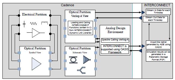
Of specific note is that Cadence and Lumerical have developed a co-simulation solution – designers no longer have to deal with the accuracy and productivity issues of attempting to manually interface testcases between separate photonic and electronic simulators.
Referring to the Analog Design Environment box in the center of the figure, Cadence Spectre manages the overall simulation timestep. Lumerical’s INTERCONNECT simulator communicates with Spectre through an interface provided by INTERCONNECT’s dynamic link libraries, part of a Verilog-A module. The Verilog-A ports represent the electrical/optical partition interface. INTERCONNECT maintains a distinct optical simulation timebase, with appropriate interpolation to return results back to the Spectre time step.
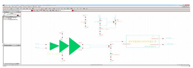
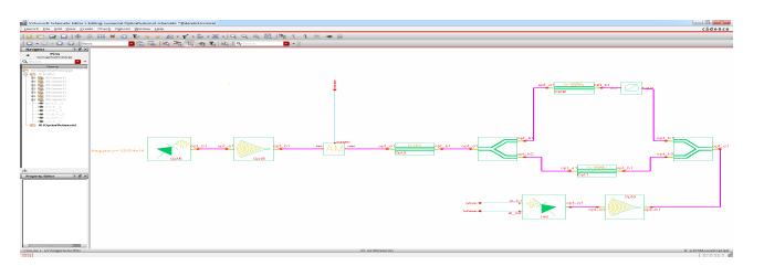
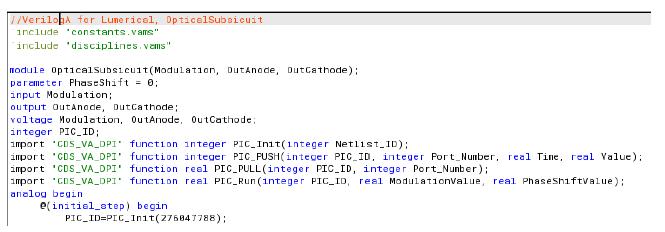
The figures below illustrate the overall flow:
- the Cadence schematic, combining electrical and optical components
- the Verilog-A view, incorporating the Lumerical interface
- the expanded optical model used by INTERCONNECT
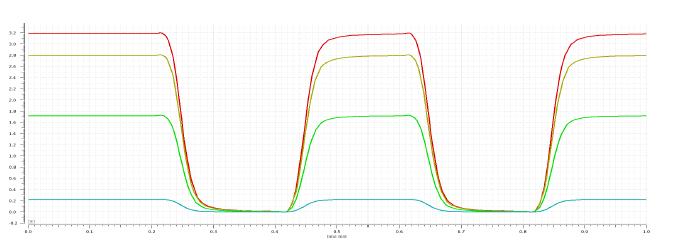
- simulation results, showing a ‘sweep’ of component parameters – in this case, the phase shift of the top branch of the waveguide in the optical model
(1) Cadence Virtuoso XL schematic
(2) INTERCONNECT optical model (expansion of the optical block in the parent schematic)
(3) Verilog-A view, integrating INTERCONNECT optical simulation
(4) simulation results, illustrating a parameter sweep
Note that this is indeed true co-simulation, with data exchange between simulators. (Verilog-A is not used as the optical model representation, as the semantics available are not well-suited to the unique characteristics of optical propagation.)
A key feature of INTERCONNECT is the use of compact models (an approach familiar to electronic designers), with S-parameter representations that span both time and frequency domains. These models have the specific advantage of enabling photonic structure parameterization through external variables, maintaining the underlying protection of IP designs.
Another productive feature of the co-simulation methodology is that familiar Spectre simulation capabilities are supported, enabling the designer to perform parameter sweeps and statistical analysis for optimization.
The integrated methodology flow for physical implementation involved the following steps:
- Virtuoso Layout XL provides support for schematic-driven layout
- PhoeniX Software’s integrated OptoDesigner provides pCell generators, specifically supporting advanced curvilinear shapes
- co-floorplanning of electronic and photonic components (including Cadence support for SiP hybrid package designs)
- layout-to-schematic back-annotation of waveguide parameters supports layout-accurate optical re-simulation
The PhoeniX pCells utilize PDK-like technology information from the foundry, to ensure that layout parameters are realizable (e.g., min/max waveguide bend radius).
An emphasis of this flow is the generation of compact model parameters from the PhoeniX pCells, for post-layout optical simulation. For example, the centerline of the waveguide is represented mathematically, which can subsequently be represented as an S-parameter matrix model.
Cadence is offering a two-day Photonics Summit and Workshop on October 19th and 20th, to provide an update on photonics technology, as well as hands-on experience with the new integrated PIC design methodology. The first day is the Summit, with an exceptional set of presentations from eminent speakers. The second Workshop day offers a set of hands-on experiences with the schematic capture, layout automation, and simulation tool flow.
Design engineers who will be expanding their scope of responsibilities to include photonic structures should attend this free summit and workshop. CAD and PDK technology engineers will also find the material extremely insightful. The link for registration on the Cadence Events site is here.
A link to the Cadence site that serves as the portal to photonics methodology development is here.
See you at the summit + workshop!
-chipguy
Share this post via:


Comments
There are no comments yet.
You must register or log in to view/post comments.