The tremendous increase in global data traffic over the past decade shows no sign of abating. Indeed, the applications for all facets of data communications are expanding, from 5G (and soon, 6G) wireless communications to metropolitan area networks serving autonomous vehicles to broader deployment of machine learning algorithms. As a result, there is a continuing need for faster signaling bandwidth among data centers – i.e., within racks, through the switch hardware, and between distant sites across a network.
There is also a greater diversity in the physical interfaces and signaling media to support communication between nodes, from long reach (LR) to ultra-short reach (USR), and from copper traces on an advanced package or printed circuit board to electro-optical conversion and optical cables.
The foundation for the increasing signal datarate support is the SerDes IP available for integration in SoCs and switch hardware (excluding the unique short-reach cases where clock-forwarded data-parallel interfaces may apply).
At the recent DesignCon conference at the Santa Clara Convention Center, Wendy Wu, Product Marketing Director in the IP Group at Cadence, provided both a historical perspective and a future roadmap outlook for serial data communications in her presentation “The Future of 224G Serial Links”. This article summarizes the highlights of her talk.
224G links are critical in the next-generation datacenter
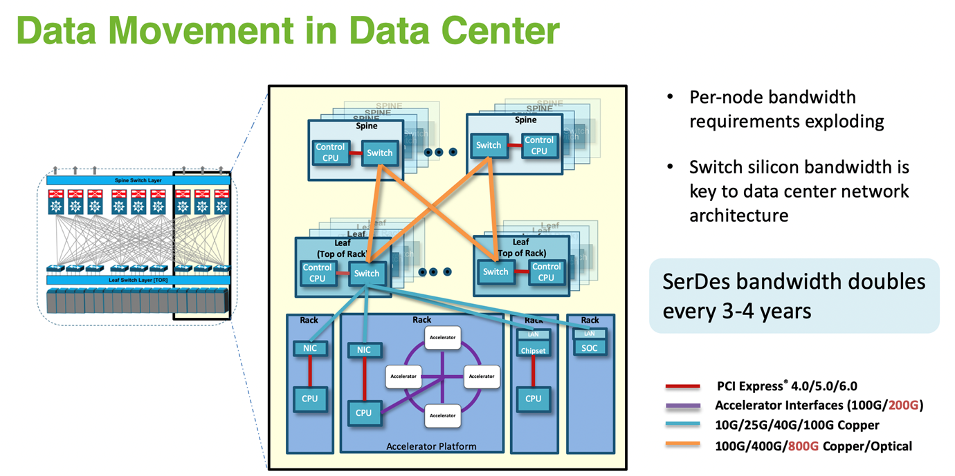
The first diagram below depicts a spine-leaf data center network architecture – the server to top-of-rack switch interface is in blue, and the rack-to-spine bandwidth interface is in orange. The spine-leaf architecture is emerging in importance, due to the increasing “east-west” data traffic between servers for distributed applications.
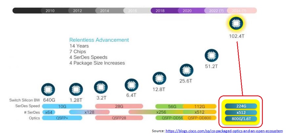
The second figure below provides a roadmap for the switch hardware, highlighting the upcoming 224G SerDes generation, in support of a 102.4T switch bandwidth. This switch design incorporates 512 lanes of 224G SerDes to provide 102.4Tbps, or 800G/1.6T Ethernet utilizing 4/8 transceiver lanes.
Switch Hardware Implementation Options
Recent “More than Moore” silicon and advanced packaging technology enhancements have enabled sophisticated, heterogeneous 2.5D implementations for the next generation of switch hardware. Wendy presented potential design examples, as shown below.
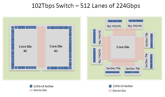
The 224G long-reach differential SerDes lanes are illustrated in blue. Extra/ultra short-reach die-to-die interfaces are shown in pink. The implementation on the right in the figure above adopts a “chiplet” approach, where the silicon technology solution for the core SoC and the 224G SerDes tiles could use different process nodes.
224G Standards Activity
There are two organizations collaborating on the standards activity for the 224G datarate definition. The IEEE 802.3df working group and the Optical Internetworking Form (OIF) consortium are focused on the definition of the 224G interface.
The goal of their efforts is to enable interoperability across the SerDes interface, encompassing: the physical media layer (both copper and fiber cable), data link layer, and link management parameters.
The OIF table below indicates some of the key targets for the 224G standard, and how it compares to previous datarate definitions.
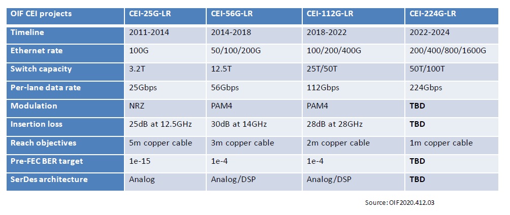
Note that there is still active discussion on several parameters – specifically, the signal modulation format and the allowable electrical channel insertion loss for the physical medium and reach target. The transition to higher datarates introduced pulse-amplitude modulation with 2 bits per unit interval – i.e., PAM4 – using four signal levels replacing the 1 bit per UI NRZ signaling used previously. The PAM definition for 224G is still being assessed, with difficult tradeoffs between:
- more bits per UI and more signal levels (e.g., PAM-6, PAM-8, or a quadrature phase and amplitude modulation)
- signal-to-noise ratios
- channel bandwidth required
- power dissipation per bit
- target bit error rate (pre-forward error correction)
- link latency
More bits per UI reduces the channel bandwidth requirements, but increases the SNR sensitivity. Continuing with PAM-4 leverages compatibility with the 112G interface, but would then require 2X the channel bandwidth (as the UI duration will be halved).
Note that the “raw” bit error rate for the high datarate PAM signaling interface is unacceptably high. A forward error correction (FEC) symbol encoding method is required, extending “k bits” in a message to “n bits” at the transmitter, with error detection and correction decoding applied at the receiver.
The table above includes a forecast for when the interoperability targets for 224G will be finalized.
Physical Topologies for 224G Links
Wendy presented several physical topologies for the 224G link (in orange), including some unique approaches, as shown below.
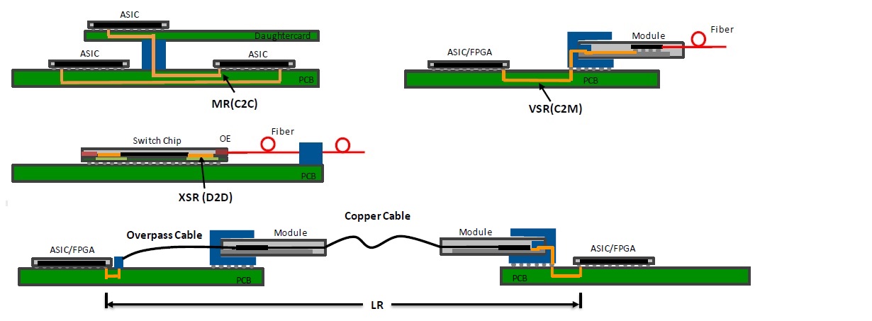
The top part of the figure above illustrates how 224G SerDes would be used in more traditional single PCB-level implementations – e.g., chip-to-chip (possibly with a mezzanine card for an accelerator, medium reach), and chip-to-optoelectronic conversion plug-in module (very short reach).
The bottom part of the figure shows two emerging designs for serial communications:
- a die-to-die, extra short reach integration of the optoelectronic circuitry in a novel 2.5D package accommodating optical fiber coupling
- the use of an “overpass cable” on the PCB itself to reach the connector, enabling a long(er) reach
The signal insertion loss for the combination of the SoC-to-overpass connector plus the overpass cable is significantly improved compared to conventional PCB traces (at the frequency of 224G PAM-4 signaling). The overpass connector is mounted on the PCB adjacent to the SoC, or potentially, integrated into an expanded package. The twin-axial overpass cable carries the differential SerDes data signal.
DSP-based Receiver Equalization
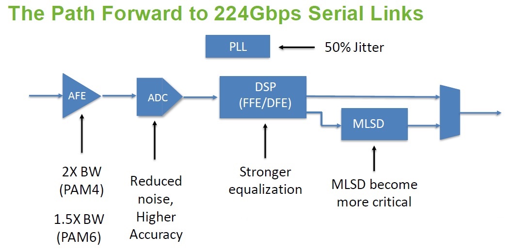
In order to double the SerDes speed from 112G to 224G, the analog front-end bandwidth needs to increase by 2X for PAM4 or by 1.5X for PAM6 to allow higher frequency component to pass through. Improved accuracy and reduced noise should to be considered for the analog-to-digital (ADC). In order to compensate for the additional loss due to the higher data rate (i.e, higher Nyquist frequency), stronger equalization might be required. This could mean more taps in the FFE and DFE. In addition, advanced algorithms such as maximum likelihood sequence detector and others will become more important at 224G. Last but not the least, because the UI is reduced by 50%, ideally the PLL clock jitter should be reduced by 50% as well.
Wendy indicated, “Cadence is an industry leader in DSP-based SerDes. There is extensive expertise in 112G SerDes IP development, spanning 7nm, 6nm, and 5nm process nodes. Customer adoption has been wide-spread. That expertise will extend to the upcoming 224G SerDes IP, as well.”
The drive for increased SerDes lane bandwidth continues at a torrid pace, with the 224G standard soon to emerge, enabling higher data traffic within and between servers.
For more information on Cadence high-speed SerDes IP offerings, please follow this link.
Also Read:
Tensilica Edge Advances at Linley
ML-Based Coverage Refinement. Innovation in Verification
Cadence and DesignCon – Workflows and SI/PI Analysis
Share this post via:


Comments
There are no comments yet.
You must register or log in to view/post comments.