At the recent Design Automation Conference, Cadence presented their methodology for incorporating performance degradation measures due to device aging into a static timing analysis flow. [1] (The work was a collaborative project with Samsung Electronics.) This article reviews the highlights of their presentation.
Background
Designers need to be cognizant of the mechanisms that contribute to degradation over the operational lifetime of a part, to ensure the overall product requirements are satisfied (e.g., FIT rate). There are both failure and degradation mechanics to address.
Failure criteria are an absolute consideration, while degradation (or “aging”) processes may result in a hard fail or have an adverse impact on circuit performance. The methodology for analyzing an aging mechanism involves an engineering assessment of the expected temperature and voltage environment, plus the switching activity likely to be applied during the part’s lifetime.
Failure Mechanisms
There is little latitude associated with the addition of ESD protect and latch-up suppression circuitry to avoid the related failures.
Time-dependent dielectric breakdown (TDDB) is an aging factor due to the “wearout” of the gate oxide dielectric. The mechanism associated with TDDB is a thermo-chemical reaction, where (weak) chemical bonds in the dielectric are broken after extended exposure to the gate electric field. The common model for TDDB is thus strongly dependent upon temperature and applied gate voltage, and may support a “soft” (resistive) followed by a “hard” breakdown current path through the gate dielectric.
The peak current density in interconnects and vias is an immediate failure process. The resistance change due to electromigration is an aging process, also strongly dependent upon temperature. (Parenthetically, some methodologies view jRMS-related electromigration wearout analysis as indicative of a hard fail, whereas other methodologies approach the PDN and/or signal interconnect resistance increase as a performance-related impact.)
Degradation Mechanisms
There are two principal device degradation aging mechanisms designers need to analyze, in terms of the potential performance impact – i.e., hot carrier injection (HCI) and bias temperature instability (BTI). These are not direct fail processes, in that they result in changes in device drive currents and threshold voltages, but not an immediate failure of the circuit to operate. They relate to the presence of carrier “trap states” at the channel interface and in the gate dielectric stack. Channel carriers may cross the potential barrier at the interface (at high electric fields) and fill the traps. The result is a change in the effective electric field at the channel from an applied gate voltage.
- HCI
HCI is commonly associated with a device operating in the saturation region – also, commonly referred to as “pinchoff” at the drain node. Carriers accelerated through the pinchoff depletion region are subjected to the gate-to-drain electric field. These carriers may originate from the channel current and/or from secondary carriers due to impact ionization. These energetic carriers may undergo a collision resulting in a vertical velocity vector, and may then trap in the dielectric stack near the drain. Hot carriers may also break chemical bonds in the dielectric stack, resulting in the generation of additional traps.
The result is a localized reduction in the gate-to-drain electric field, as part of the electric field now terminates on the trapped charge. This is typically modeled as a reduction in the effective channel carrier mobility. (Note that if the device is used as a bidirectional pass gate, this drain node now becomes the source – a model that alters the threshold voltage rather than the carrier mobility may be more appropriate.)
For logic circuits, devices are operating in the saturation region only during a brief interval of a signal transition. (For analog/mixed-signal circuits, devices biased in saturation are subjected to greater HCI exposure.) As a result, logic performance degradation is commonly associated with BTI.
- BTI
The bias temperature instability mechanism is present when the device is operating in the linear region. This occurs when a logic device is “on” and has completed a signal transition.
Channel carriers enter the dielectric stack and fill trap states. BTI manifests as an adverse shift in the device threshold voltage – i.e., an increase in the absolute value of Vt for both nMOS and pMOS devices. Negative BTI (NBTI) refers to the pMOS device Vt shift, due to the negative gate-to-channel electric field direction; pBTI refers to the nMOS device Vt shift.
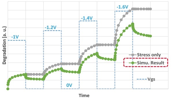
The delta in the threshold voltage eventually saturates over time as trap states are filled. Note that BTI models also include a (partial) recovery in the Vt shift for the time period when the device gate-to-channel electric field is reversed, as depicted below. [2]

As the BTI mechanism is present whenever a logic gate is quiescent, the Vt shift contributes to significant performance degradation over a part’s lifetime.
Static Timing Analysis Methodology with Aging
The simplest method to modeling aging effects would be to apply a multiplicative “derate” to the target cycle time. In short, the “fresh” cycle time used during design timing closure would be multiplied by a conservative aging factor and released with the reduced frequency spec – i.e., a “guardband” approach.
Alternatively, a more sophisticated method would be to apply a cell instance-specific delay calculation for aging to an STA flow. The individual cell delay arcs would reflect a (voltage and temperature) environmental assumption over the circuit lifetime. This method requires a cell library characterization strategy that expands upon the traditional model of:
delay_arc = f( PVT, input_slew, output_load)
to include new dimensions, reflecting the aging delay value. The figure below depicts the Cadence methodology for cell characterization and aging-aware STA.

The characterization strategy requires adding delay values for different combinations of Vt shifts due to BTI of individual devices. Spice aging models are provided by the foundry.
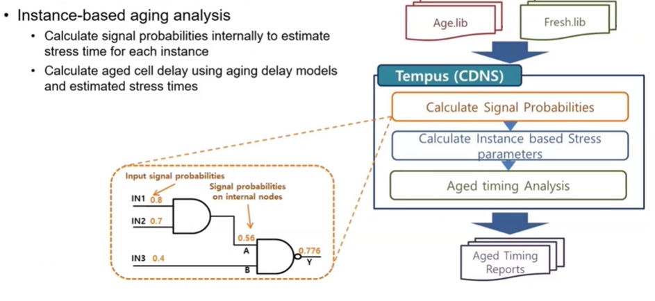
The static timing analysis flow is depicted on the right side of the figure above. An additional input to the aging-aware STA flow is a description of the (piece-wise) expected voltage and temperature conditions which individual blocks will experience over the part lifetime. The methodology for calculating the duration for which each device is subjected to forward and recovery BTI stress is based on signal probability measures, as illustrated in the figure below.

As an example, for the 2-input NAND gate in the figure, if pin A has a (0,1) probability of (0.44,0.56), and pin B has a (0.6,0.4) probability, the gate output will have a (0.224,0.776) probability to apply to its fanout, derived from the calculation (0.56*0.4, 1 – 0.56*0.4).
An alternative approach would be to apply signal value duty cycles from extensive (gate-level) workload simulations. The probabilistic approach is simpler, yet it may not reflect extended periods of operation in a specific quiescent state.
To illustrate the flow, Cadence collaborated with Samsung on a 5nm process node design example. Using the Samsung aging model design kit for library cell characterization, STA was pursued for a core-level design. Then, 500 paths were selected for a detailed Spice-based aging delay simulation. The STA versus Spice comparison data is shown below.

Summary
Designers need to evaluate performance degradation effects due to BTI stress over a part’s lifetime. Using a uniform guardband multiplier is could be quite inaccurate, as it would not be representative of the varying stress/recovery characteristics of (instance-specific) circuit activity.
For more information on the aging-aware STA flow from Cadence, please follow this link.
References
[1] Amin, C., et al., “Aging-aware Static Timing Analysis”, DAC 2021.
Also Read
Scalable Concolic Testing. Innovation in Verification
More Than Moore and Charting the Path Beyond 3nm
Topics for Innovation in Verification
Share this post via:


Comments
There are no comments yet.
You must register or log in to view/post comments.