Almost everything that we do in chip design and verification was invented to raise the abstraction above schematics and polygons. Register-transfer-level (RTL) design, functional simulation, logic synthesis, floorplanning, and more fall into this category. Even the notion of binary circuits is an abstraction. Underneath all this, the real world is analog, and the fundamental effects of electricity and silicon can’t be ignored or abstracted away.
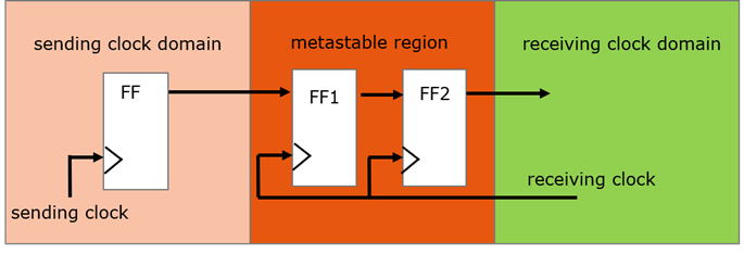
One of these inconvenient truths is metastability, which can occur wherever a signal crosses between flip-flops on asynchronous clocks, called a clock domain crossing (CDC). If the input to the receiving flip-flop changes too close to its active clock edge, the flip-flop can take an indeterminate value before settling to a one or zero. If the flip-flop feeds the indeterminate value to downstream logic, the circuit may produce incorrect results.
Since there’s no way to avoid metastability, best practices for CDC design require that the downstream logic receives only valid values. The classic way to ensure this is to use a synchronizer consisting of two flip-flops on the receiving clock. If properly designed, there is a very high probability that the signal will have settled before it is clocked into the second flip-flop. Thus, only valid values are passed on to the rest of the circuit.

Multi-bit signals such as data buses require another approach since the bits may have different delays and an incorrect data value may be loaded into the receiving flip-flops. The best way to handle this is a handshake synchronizer, which creates a multi-cycle path (MCP) for the data bits so the inputs to the receiving flip-flops will be stable by the time the values are clocked in. This ensures that there is no metastability.

One common location for CDCs is the control and status registers (CSRs) used by low-level software to control and monitor chip hardware. CSR blocks have a software interface from which programs running on host systems (such as device drivers) or code running on the chip’s own embedded processors can write or read the registers. The software interface and register blocks themselves are usually in the system bus clock domain.
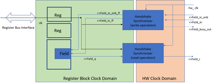
CSR blocks also have a hardware interface from which the rest of the chip can read or write the registers. The hardware uses this interface to read configuration values, communicate status back to the software, handshake with the software, and exchange data. Since the rest of the chip is almost always on a different clock than the system bus, there is a CDC that must be handled properly. Typically, two handshake synchronizers are used, one for the write path and one for the read.

Agnisys provides a pushbutton solution for clock domain crossings related to register blocks. Our IDesignSpec™ Suite helps chip architects and engineers create an executable specification for CSRs and automatically generate outputs for software and hardware teams. This includes generating the RTL code for the register block (in VHDL, Verilog, SystemVerilog, or SystemC) plus a bus slave and decode logic specific to the system bus protocol (AHB, APB, AXI, TileLink, or proprietary).
If the registers are in a different clock domain than the system bus, our solution also generates RTL for all the synchronization logic plus assertions for use in formal CDC verification. We support all three types of synchronizers discussed plus other options, including two-level flip-flops, mux, handshake, async FIFO synchronizers, and custom synchronizer blocks. We also handle cases in which the register block is in its own separate clock domain, distinct from the system bus and the rest of the hardware design.
We have many users who have benefitted from this automation. They do not need to worry about CDCs at all: they simply tell us their preferred synchronizer style and we generate everything for them. We have a lot of experience with CDCs and synchronization, and we are sharing our expertise with the rest of the industry. We are actively participating in the new Clock Domain Crossing Working Group within the Accellera Systems Initiative, focused on creating a standard for CDC abstraction models.
Should you want to have a discussion about clock domain crossing or any other design challenges, or would like to see a demo of the latest enhancements to our IDesignSpec Suite please contact us directly.
Agnisys is here to help you accelerate your IP/SoC front-end development with the industry’s leading Golden Executable Specification Solutions.
WEBINAR: An Introduction to Correct-by-Construction Golden Specification-based IP/SoC Development
Also Read:
ISO 26262: Feeling Safe in Your Self-Driving Car
DAC 2021 – What’s Up with Agnisys and Spec-driven IC Development
Share this post via:


Silicon Insurance: Why eFPGA is Cheaper Than a Respin — and Why It Matters in the Intel 18A Era