 I was at Mentor’s u2u (user group) meeting and one of the keynotes was by Ivo Bolsens of Xilinx. The other was by Wally Rhines and is summarized here.
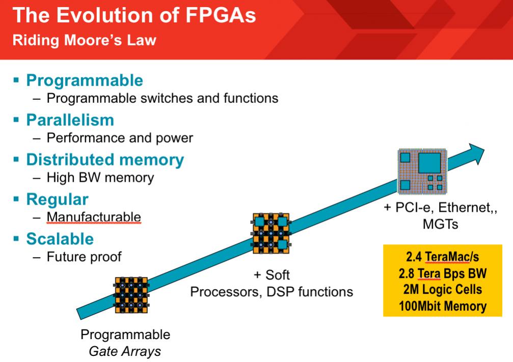
Ivo started off talking analogizing SoCs as the sports-cars of the industry (fast but expensive), and FPGAs as the station wagons (not cool). In fact he even said that when Xilinx started an FPGA was a pretty silly idea. When everyone was optimizing every square micron of area, take 20 gates to do the work of 1. But, of course, each process generation makes the idea less silly. A crossover SoC is a design that takes some of the integration ideas from SoCs, couples them with the flexibility and time-to-market from programmable logic along with the financial constraints and application focus of ASSPs. Like a crossover vehicle which is really an SUV built on a car chassis.
 Of course people have tried to do this sort of thing before. Remember structured ASICs like LSI Logic’s RapidChip. Or multi-chip modules which suffered from excessive power consumption and the signals between chips being too slow (not much better than going off chip across a PCB).
There are two technologies that Ivo sees as being the foundation of crossover chips. One is the monolithic CPU+programmable-logic. The other is 3D system in package, or mostly what has come tb be called 2.5D systems, flipping microbumped die onto a silicon interposer. More about that is also here and see the wiki on 3D chips here. The main thing about both of these approaches is that it tightens the connection between CPU and FPGA.
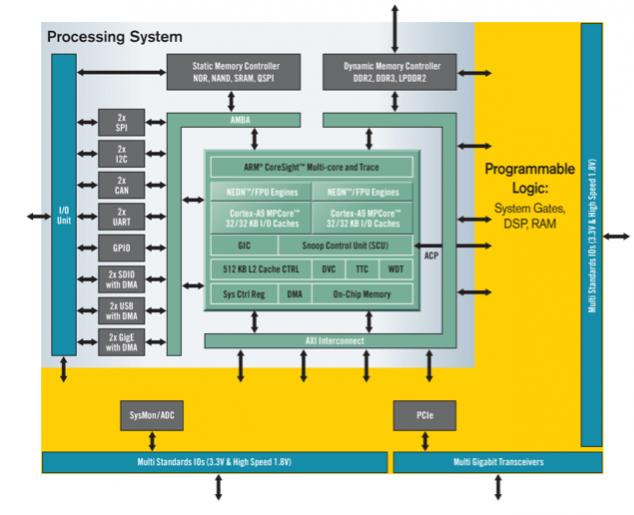
So Xilinx created the Xinq series (and not just to get the all time high score at Scrabble) containing:
 Dual ARM Cortex-A9 MP
- Integrated ARM memory controllers and peripherals
- Integrated on-chip memory
- 28nm Xilinx state-of-the-art FPGA
- Flexible array of I/Os: serial tranceivers, analog-to-digital converter inputs
So it is blend between a CPU and an FPGA. Or, another way of looking at it, it is an SoC with just the CPU subsystem realized in custom silicon, and everything else realized by programming the FPGA. By adding cache coherency between the processor cores and the FPGA you get automatic cache-to-cache data movement, low latency access to FPGA data from the CPU and vice-versa and no need for repeat cache flushing.
Standards are clearly going to be important in the crossover world. Standards for FPGA-CPU interconnect and protocols. Rules for TSV, microbumps and interoperability of silicon from different companies.
In conclusion:
- FPGA landscape will change
- Heterogeneous multicore and 3D are key
- Standards are key enablers
- New business models will emerge


Comments
0 Replies to “Ivo Bolsens of Xilinx and Crossover Designs”
You must register or log in to view/post comments.