PCB designers have been using manual routing for decades now, so when is it time to consider adding interactive routing technologies to become more productive? Manually routing traces to connect components will take time from a skilled team member and involves human judgement that will introduce errors. When a design change comes in, then iterating the PCB layout manually can be a slow process, leading to project delays. Growing complexity in PCB designs caused by higher component density, and boards using multiple layers really challenge manual routing approaches. Finding PCB designers with expertise to complete manual routing efficiently can be another burden.

PCB automation tools can quickly connect components, which saves designers time and effort. A designer can then spend their time on other challenges, like signal integrity validation, lowering interference and meeting design constraints. An automated tool will produce consistent results, lowering errors. With automation the trace widths are more uniform, clearances are maintained, preventing the need for revisions. Even when a design change arrives, the automated routing approach tackles the task quickly. The learning curve for automation tools is brief, so payback happens quickly. Automation improvements depend on design complexity, routing automation quality, designer skills and project requirements.
The industry isn’t at the level of full automation for PCB routing, so don’t expect a push-button flow for all designs. A PCB design may have unique and complex design constraints and requirements that would make an autorouter ineffective. Component placement, signal integrity (SI), thermal management, and EMI/EMC compliance, can all require manual routing. Analog components and high-speed signals may demand manual routing to achieve the precision required. Some autorouters introduce errors, causing manual rework and unforeseen delays. Learning a new autorouter can require time to become proficient, especially if the tool has too many arcane settings. Achieving a specific PCB layout style may not be possible using an automated tool. Some combination of manual and automated routing will typically yield the best results.
PCB designers are still required to solve issues like the design concept and specification, selecting the proper components, performing signal integrity analysis and optimizing high-speed designs, routing the most critical signals, managing the thermal goals, complying with EMI/EMC requirements. Humans are also best suited to make complex trade-offs between cost, performance, size, and manufacturing. Yes, automation tools will speed up parts of a PCB project, while manual methods will remain for the more abstract tasks.
PADS Professional
Siemens has created a sketch path feature in the PADS Professional tool that enables a PCB designer to achieve high design quality and high completion rates in less time compared to manual routing. Users can route individual traces or hundreds of single-ended differential pairs. Plus, this technology will automatically improve pin escapes during routing while avoiding the use of vias.
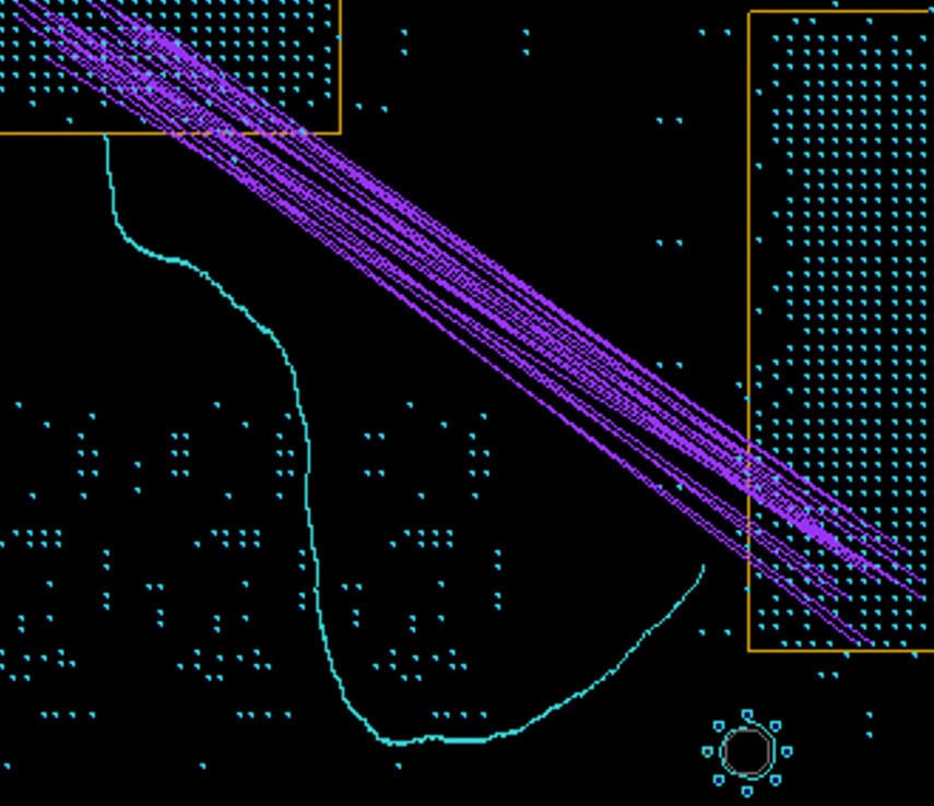
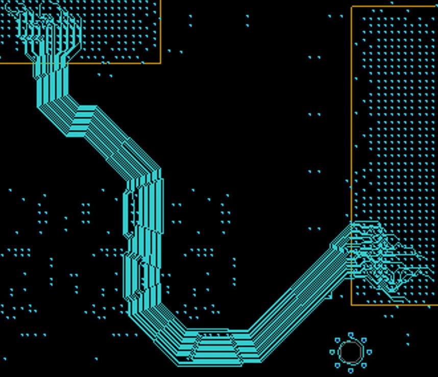
Sketch routing allows a PCB designer to automatically fan out, untangle, and route specific nets with hand-route quality, as shown below.


With sketch routing a designer quickly draws where routing should go by selecting an unrouted net and “dragging” the cursor on the rough path they’d like. Then the PADS Professional sketch router will automatically complete the routing one net at a time, all with little or no cleanup required. Even using components like BGAs, the sketch routing completes without using extra vias, achieving typical completion rates above 90 percent. The sketch routing in PADS Professional uses dynamic push-and-shove, along with real trace routing.
Summary
The old maxim that time is money still rings true for PCB projects today. Manual routing has been done for many years, yet it can take too much time and likely requires an experienced user. The sketch router feature in PADS Professional is a capable method to automate many routing tasks that used to be done manually, so your project can complete in less time, with fewer experts and higher quality.
Read the 8 page eBook online from Siemens.
Related Blogs
Share this post via:


Comments
There are no comments yet.
You must register or log in to view/post comments.