IC designs have physical verification applications like Layout Versus Schematic (LVS) at the transistor-level to ensure that layout and schematics are equivalent, in addition there’s an Electrical Rules Check (ERC) for connections to well regions called a soft check. The connections to all the devices needs to have the most consistent voltage signals. Therefore, the path should be through the Metal layers to reduce resistance and factors like IR Drop. Detecting connections thought other materials–like Wells–in mandatory. Soft-Checks are the method most commonly employed to detect this situation. The Calibre product line from Siemens is the most popular tool for DRC and LVS checking, so I read a technical paper from Terry Meeks to learn more about soft checks.
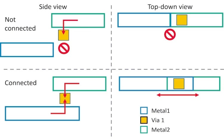
Connecting two metal layers in an IC layout requires precise alignment of both metal layers and the via layer. Here’s a comparison using both a side view and top-down view where the first example is not connected, because Metal1 and Metal 2 are not overlapping, while the second example is connected properly.
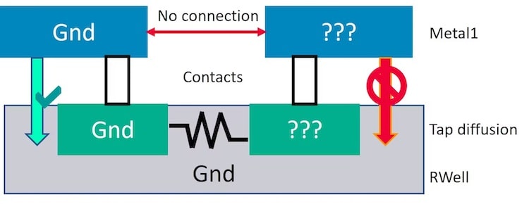
We want our ERC tool to identify well connectivity errors during soft checks, so that they can be fixed. The following IC layout has a well connectivity error and is shown from the side view, where the Metal1 signal texted as Gnd is connected a diffusion region called a tap diffusion. On the right-hand side is another Metal1 layer with a tap diffusion, but this connectivity creates a high-resistance path in the Rwell to Gnd, and is flagged as an error by the soft check.
Another example of soft connectivity error happens in the IC layout below where we can apply only one name per polygon. The digital power net VDD cannot coexist with the analog power net AVDD, and we need to separate these into two shapes. Soft checks help to flag these issues.

An IC layout with both digital and analog power supplies can become rather complex to layout properly, so it’s even more important to have soft checks.

Soft checks are included during your LVS runs, and with Calibre nmLVS there’s a report of soft check results, which can then be viewed using the Calibre RVE viewer.
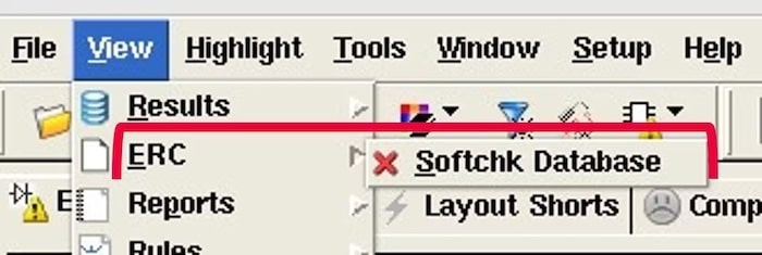
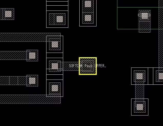
Clicking on RVE results tells you which cell has the soft check error, the net names, upper and lower names, and other properties. This info helps to pinpoint what to fix in the IC layout. Clicking on a lower layer like a PWell for a soft check error displays the geometry in yellow.
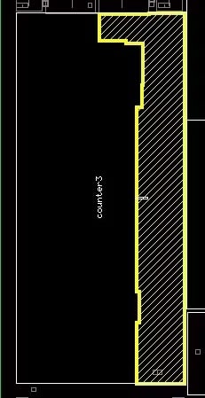
For the same soft check error, clicking on the upper layer shows:
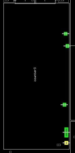
During debug you can also show all the upper layer shapes, the green shapes are the selected net upper layer shapes, while yellow is the rejected net upper layer shape.
Debugging soft check errors with RVE involves clicking on the connectivity of selected and rejected nets. A Net Info windows reveals details like which layers are involved, and if shapes are missing connectivity. Looking at which ports are connected to a net reveal if there’s missing VDD or GND errors. This example shows that net 18 is rejected, because it’s missing connectivity to Metal1.

Summary
LVS checks are mandatory to ensure that an IC has an error-free layout, and soft checks are part of your LVS checks. There’s a proven debugging flow from Siemens in their Calibre nmLVS tool that uses RVE to help layout designers quickly identify soft check failures, so that designers can make fixes and re-verify until all checks are passing. Siemens has written a technical paper for reading online, Detecting and debugging soft check connectivity errors.
Related Blogs
- Getting the most out of a shift-left IC physical verification flow with the Calibre nmPlatform
- Building better design flows with tool Open APIs – Calibre RealTime integration shows the way forward
- Calibre: Early Design LVS and ERC Checking gets Interesting
Share this post via:


Comments
There are no comments yet.
You must register or log in to view/post comments.