Semiconductors sit at the heart of the electronics revolution, and the scaling enabled by Moore’s law has had a transformational impact on electronics as well as society. Traditionally, the relationship between semiconductor companies and their customers has been a function of the volume driven by the customer. In very high-volume markets such as the consumer marketplace, large numbers of staff from semiconductor companies work with their system counterparts to effectively co-design the system product.
However, for non-consumer markets, the semiconductor interface largely consists of datasheets, websites, and reference designs. Surprisingly, this picture has not changed much since the 1980s. Meanwhile, in the intervening decades, Moore’s law has enabled the construction of much more complex devices with incredible flexibility and the support of higher levels of abstraction (AI, SW, and others). Yet, the primary method of communication between semiconductor companies and their system customers remains English text, and this interface is breaking down.
In this article, we will discuss the changing nature of System PCB design for non-consumer system designers, the current organization of the electronics design chain, the tremendous gaps being created in the current situation, and the outlines of a solution.
System PCB Design:

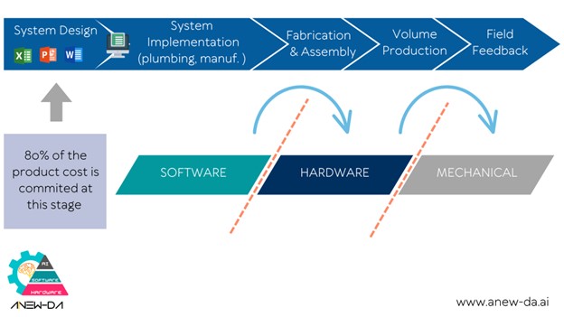
Figure 1: The Modern System PCB Design Process for non-consumer
As figure one shows, in this non-consumer electronics flow, the electronic design steps consist of the following stages:
- System Design: In this phase, a senior system designer is mapping their idea of function to key electronics components. In picking these key components, the system designer is often making these choices with the following considerations:
a. Do these components conform to any certification requirements in my application?
b. Is there a software (SW) ecosystem which provides so much value that I must pick hardware (HW) components in a specific software Architecture?
c. Are there AI/ML components which are critical to my application which imply choice of an optimal HW and SW stack most suited for my end application?
d. Do these components fit in my operational domain of space, power, and performance at a feasibility level of analysis.
e. Observation: This stage of design determines the vast majority of immediate and lifecycle cost. For a semiconductor company, if you do not participate at this level of design, you may be locked out for years.
f. Today, this stage of design is largely unstructured with the use of generic personal productivity tools such as XL, Word, PDF (for reading 200+ page data sheets), and of course google search.
System Implementation: In this phase, the key components from the system design must be refined into a physical PCB design. Typically driven by electrical engineers within the organization or sourced by external design services, this stage of design has the following considerations:
a. PCB Plumbing: Combining the requirements of key components with the external facing aspects of the PCB is the job at this stage of design. This often involves a physical layout of the PCB, defining power/gnd/clk architecture, and any signal level electrical work. This phase also involves part selection, but typically of the low complexity (microcontrollers) and analog nature. Today, this stage of design is reasonably well supported by the physical design, signal integrity, and electrical simulation tools from the traditional EDA Vendors such as Cadence, Zuken and Mentor-Graphics. Part Selection is reasonably well supported by web interfaces from companies such as Mouser and Digikey. However, this stage of design is highly susceptible to a total solution package from the high-level system design phase. If someone offers a subsystem which solves a real system design problem and includes PCB Plumbing, there is no reason to recreate the PCB plumbing.
b. Bootup Architecture: As the physical design is being put together, a bootup architecture which typically proceeds through electrical stability (DC_OK), testability, micro-code/fpga ramp up, and finally to a live operating system. Typically, connected to this work are a large range of tools to help debug the PCB board. The combination of all of these capabilities is referred to as the Board Support Package (BSP). BSPs must span across all the abstraction levels of the System PCB, so today, often they are “cobbled” together from a base of tools with parts sitting on various websites.
This design flow is a contrast from the System PCB flow of the 1980’s where the focus of a System PCB was largely to build a function (example: sliced CPU). The actual semiconductors used to build the function were of moderate complexity and the communication mechanism of a datasheet was adequate. Today, the job of a System PCB designer has dramatically shifted to managing complex fabrics within complex HW/SW ecosystems (AI is coming next).
Yet, the primary method for communication of technical information is still with large volumes of English sitting in datasheets and websites. Further, most of the non-consumer marketplace has requirements for long lifecycles (LLC) which are also at odds with the core of the consumer-focused semiconductor chain.
Moreover, the organization of the distribution and support network from semiconductor companies is not very helpful in resolving this major issue.
Current Organization of the Electronics Design Chain:

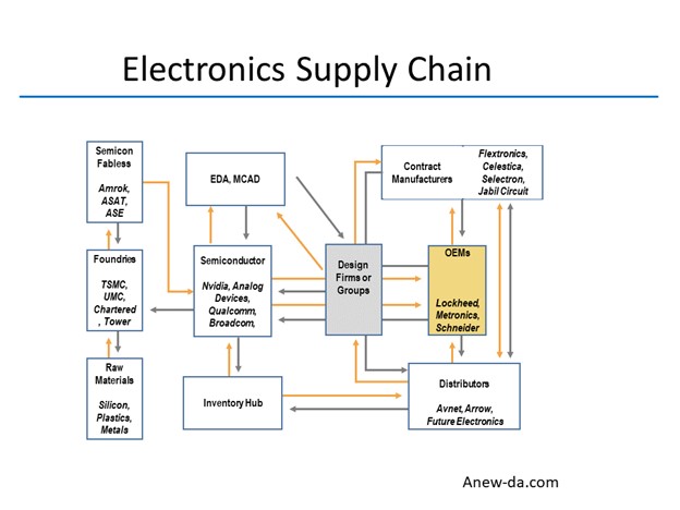
Figure 2: Electronics Design and Supply Chain
Over the decades, the electronics supply chain has evolved to a complex web of companies which connects semiconductor makers to the end customers. The major players in the ecosystem are: the semiconductor companies themselves, Electronic Manufacturing Services (EMS), Electronics Distributors, and electronic design automation companies. Let us examine each and their roles for System PCB customers.
- Semiconductor Companies: Semiconductor companies with significant focus on the non-consumer market segments (Texas Instruments, Analog Devices, etc) often have tens of thousands of product SKU’s. As previously discussed, from a distribution point of view, semiconductor companies focus on high volume customers. These are the customers which get the attention of their application engineering organization. For the broad market, broadcast mechanisms such as websites are used, and semiconductor companies try to enable distributors to support the broader marketplace. As part have become more complex, the semiconductor will often offer helper widgets (software, spreadsheets, websites) to aid in the usage of their parts. However, since there is no unified coherent structure, System PCB designers must face a dizzing range of tools/widgets/spreadsheets.
- Electronics Distributors: Companies such as Avnet and Arrow provide a marketing and distribution function for semiconductor manufacturers. In the context of LLC, they can provide inventory services and often provide a layer of other support services. Of course, their ability to support semiconductor parts is limited by the medium of communication from semiconductor companies (datasheets, websites, reference designs) to them.
- EMS Companies: EMS companies such as Flextronics and Jabil Circuit engage with LLC customers to assemble and build the Printed Circuit Boards (PCBs). Originally, many EMS companies were spinouts from traditional OEMs such as IBM or HP who wanted to shed low-margin business (EMS companies have margins in the low single digits). Over time, EMS companies have moved from serving consumer customers to LLC customers. LLC customers are generally low volume and benefit from the aggregation manufacturing function provided by EMS companies. However, much like electronic distributors, EMS companies are limited by the medium of communication from semiconductor companies.
- EDA Companies: Electronics Design Automation (EDA) companies such as Cadence Design Systems, Synopsys, and Mentor Graphics (Siemens) provide the key design tools and some level of the design and verification IP required to build electronic systems. Today, the vast majority of the business in EDA is focused on semiconductor design. Even the “systems” divisions of these companies focus on issues such as HW/SW codesign in the context of System-on-chip semiconductor implementations. In the System PCB world, the core design tool set consists of traditional PCB physical design tools (Orcad, Zukan, Pads, Altium), independent design tools from FPGA vendors, and many chip specs off of semiconductor company websites. Today, EDA companies do not offer anything that helps with the complex system PCB design process.
Overall, the current sales, distribution, and support structure enabled by semiconductor companies creates even more distance between themselves and their system PCB customers.
Implications of the gap between Semiconductor companies and their System Customers:
The current situation is not good for anyone. For semiconductor companies, the current situation has the following drawbacks:
- Lack of market Insight: The distance between semiconductor companies and their customers is a tremendous loss of information relative to understanding issues with current products, true differentiation for their products, and the potential for future product integrations.
- Communicating Differentiation: Semiconductor companies have the ability to integrate functionality, build supporting tools to take advantage of this functionality, and build whole solution stacks. However, the current data-sheet/website method of technical knowledge delivery makes it very difficult to communicate this value. This is especially the case if a combination of chip functionality and SW programmability provides unique value.
For system PCB customers, the current situation faces the following drawbacks:
- Complexity: The key issue is managing the massive complexity of information coming from semiconductor companies. Two-hundred-page data-sheets are not unusual. This is the reason that the biggest indicator of which chip a system PCB designer will use is: “Have they used the chip before?” This is unfortunate because compelling solutions are often missed.
- Support: Most system PCB customers are in a situation where they cannot count on any real access to technical support resources unless they can drive high volumes. For everyone else, understanding complex semiconductor systems must be done without any real direct support. This is one of the reasons that independent discussion groups are popping up in the System Design community.
- Constraint Management: The information on semiconductors sits on datasheets and a whole host of websites which also contains increasing amounts of soft information (which includes OS, driver, supporting tool updates, AI stack etc) which is dynamically changing. This is tedious and utterly inefficient and a place of great pain for System PCB customers.
Overall, System PCB customers face a chaotic, complex, and dynamic semiconductor marketplace. Their “tools” for managing this process are Excel, word, and google search. This is an inefficient and painful situation which results in a great headwind for product development velocity. This is bad for everyone involved in System PCB companies, Semiconductor companies, and perhaps most importantly society.
What are the outlines of a solution?
The solution to complexity has always been the addition of organization, structure, and automation. These are the hallmarks of the EDA industry. There is a need for an EDA tool which manages the System PCB design. The key characteristics of such an EDA tool would be:
- System PCB Design Flow: The EDA tool would follow the modern system design process. Specifically, the flow of certification, constraints, respect for AI/SW ecosystems, and more.
- Rationalization and Organization of Semiconductor Function: System PCB designers think in terms of function, and semiconductors must be organized in this manner.
- Integration of reference design and helper tools: Within the context of the above step, reference designs and helper tools can be organized rationally
All the above is very doable with a little cooperation between EDA, System PCB, and Semiconductor companies. The result would be a massive acceleration in system design productivity, which is good for everyone involved.
Acknowledgements: Special thanks to Anurag Seth for co-authoring this article.
Also Read:
Balancing Analog Layout Parasitics in MOSFET Differential Pairs
STOP Writing RTL for Registers
The CHIPS and Science Act, Cybersecurity, and Semiconductor Manufacturing
Share this post via:


Musk’s Orbital Compute Vision: TERAFAB and the End of the Terrestrial Data Center