My first transistor-level IC design job was with Intel, doing DRAM designs by shrinking the layout to a smaller process node, and it also required running lots of SPICE runs with manually extracted parasitics to verify that everything was operating OK, meeting the access time specifications and power requirements across PVT corners. I’d do a SPICE run, and show the waveform and timing results to a senior circuit designer, and then he’d ask for the schematics and say, “Go and make this change, then rerun SPICE again.” What a slow and laborious process it was to migrate a high-volume memory part. Eventually I learned the art and science of DRAM design, and then became a senior circuit designer, responsible for eyeballing other designers schematics, reviewing their waveforms, and telling them, “Go and make this change, then rerun SPICE again.”
The EDA industry has paid attention to the challenges of transistor-level circuit designers over the years and has come up with something beyond just running lots of SPICE circuit simulations, and that tool category is known as static checking, which is something that complements what SPICE can tell you. A new white paper from Siemens EDA was just released on static checking, and I’ll give you an overview of what static checks can help you quickly verify.
Power-Intent Checks
IP blocks within an SoC can employ many power domains, and that requires some transistor-level design control with:
- Voltage regulators
- Header and footer switches
- Level shifters
- Isolation cells
- State retention cells
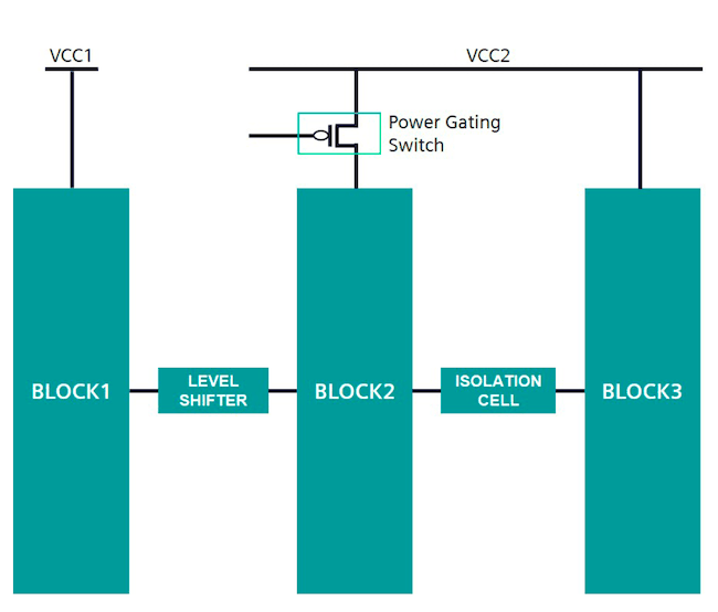
In the following block diagram the circuit designer needs to place and verify that there is a level shifter between the power domains connected to VCC1 and VCC2, transistors with thick oxide are connected to the high voltage supply, and that an isolation cell is placed between Block 2 and 3, because Block 2 has gated power.

A static checker can automatically detect every power domain crossing in a chip, and verify that level shifters and isolation cells are properly placed. You really want to be using a transistor-level verification tool for tricky tasks like this to ensure thorough verification. Catching and fixing a power intent bug before tape out makes economic sense.
ESD Protection Verification
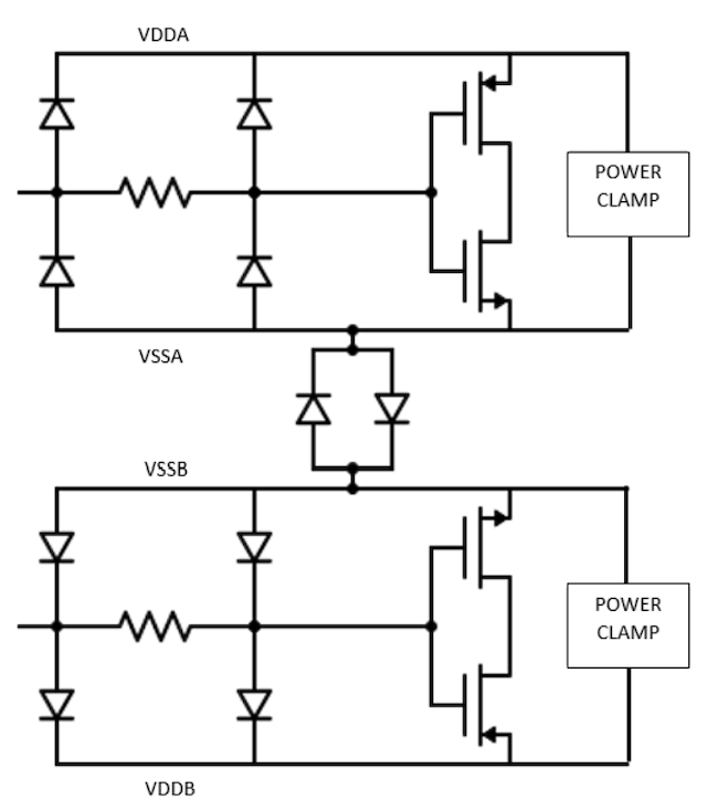
I remember placing DRAM chips onto a tester during characterization, and we always wore a conductive strap connected to the tester, which prevented the build up of Electro Static Discharge (ESD) while walking on the carpet, that created a large voltage that potentially damaged the IC as current flowed into the chip. IO cells on a chip using multiple power domains have special diodes to shunt the high ESD currents away from rest of the chip.

A static checker can find all of these ESD elements, including parasitic resistances and capacitances, and calculate ESD safety limits much faster than running an exhaustive number of SPICE simulations. Vias on interconnect layers in the ESD path can be statically checked for electromigration compliance.
Voltage-Aware Spacing Checks
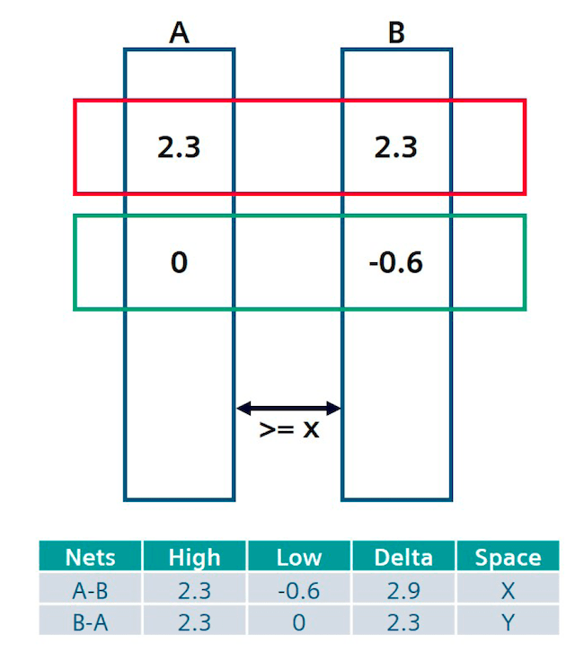
There’s a reliability concern called Time-Dependent Dielectric Breakdown (TDDB), where the allowed spacing of wires is dependent of the voltages of the wires.

A typical DRC tool doesn’t know about voltages, and trying to run dynamic SPICE simulations on a full chip isn’t practical, so the smarter approach is using a tool that can do static voltage propagation and topology checks for TDDB.
Analog layout-dependent checks
AMS designers know about taking layout precautions to ensure robust operation, like:
- Device layout symmetry
- Current orientation matching
- Dummy device insertions
- Common centroid and pitch between devices
- Electrical parameter matching
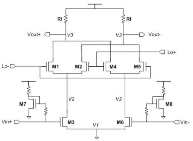
In the following schematic for a fully differential mixer the layout designer needs to use symmetry between:
- M1, M2, M4, M5
- M3, M6
- M7, M8
- RI

Small layout differences can impact performance, while a static checker can quickly identify any layout dependent violations.
Summary
Yes, SPICE circuit simulation is still heavily used for transistor-level IP design and verification, but using advanced, FinFET process nodes, there are so many more effects to verify now that it makes sense to add a static checker to ensure that your designs are meeting power intent, ESD protection, voltage-aware spacing, and analog layout-dependent effects. Using the right tool for the right task makes the life of a chip designer less stressful, and ensures that silicon will perform to spec, and operate reliably.
The full white paper is online here.
Related Blogs
- Configuration Environment is Make-or-Break for IC Verification
- Saving Time in Physical Verification by Reusing Metadata
- Beyond DRC and LVS, why Reliability Verification is used by Foundries
- Foundry Partnership Simplifies Design for Reliability
- Electrical Reliability Verification – Now At FullChip
- Silicon Creations talks about 7nm IP Verification for AMS Circuits


Comments
2 Replies to “Transistor-Level Static Checking for Better Performance and Reliability”
You must register or log in to view/post comments.