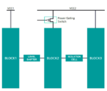
Custom and Analog-Mixed Signal (AMS) IC design are used when the highest performance is required, and using digital standard cells just won’t meet the requirements. Manually sizing schematics, doing IC layout, extracting parasitics, then measuring the performance only to go back and continue iterating is a long, tedious… Read More
Tag: ams verification
Transistor-Level Static Checking for Better Performance and Reliability
My first transistor-level IC design job was with Intel, doing DRAM designs by shrinking the layout to a smaller process node, and it also required running lots of SPICE runs with manually extracted parasitics to verify that everything was operating OK, meeting the access time specifications and power requirements across PVT … Read More
Cadence Update on AMS Design and Verification at #55DAC
As a blogger in the EDA industry I get more invitations to meet with folks at DAC than I have time slots, so I have to be a bit selective in who I meet. When the folks at Cadence asked me to sit down and chat with Mladen Nizic I was intrigued because Mladen is so well-known in the AMS language area and he’s one of the authors of, The Mixed-Signal… Read More
AMS Design, Layout and Verification @ #50DAC
Competition in EDA is absolutely necessary in order for the fabless semiconductor ecosystem to thrive. AMS tools with a low learning curve, high interoperability, and a powerful user interface improve design team productivity and enable a low total cost of ownership. That is why Tanner EDA has shipped over 33,000 licenses of … Read More
USB 3.0 PHY Verification: how to manage AMS IP verification?
Very interesting question from Zahrein in this thread: “how to manage an embedded USB 3.0 PHY Verification”? To clearly position the problem, Zahrein need to run the RTL verification of a complete SoC integrating an USB 3.0 function, that is the Controller (digital) and the PHY (Analog Mixed Signal) embedded in the SoC. The question,… Read More


