You are currently viewing SemiWiki as a guest which gives you limited access to the site. To view blog comments and experience other SemiWiki features you must be a registered member. Registration is fast, simple, and absolutely free so please,
join our community today!
The meaning of the word “Veloce” is “blazing fast”. It is the inspiration behind the name of the Ansys VeloceRF electromagnetic (EM) passive device synthesis platform that has been a favorite among RF and high-speed integrated circuit (IC) designers for more than 15 years. VeloceRF is a name that designers automatically connect… Read More
My first transistor-level IC design job was with Intel, doing DRAM designs by shrinking the layout to a smaller process node, and it also required running lots of SPICE runs with manually extracted parasitics to verify that everything was operating OK, meeting the access time specifications and power requirements across PVT … Read More
In RF designs Low Noise Amplifiers (LNA) play a critical role in system operation. They simultaneously need to be extremely sensitive and noise free, yet also must be able to withstand strong signal input without distortion. LNA designers often struggle to meet device performance specifications. Their task is further complicated… Read More
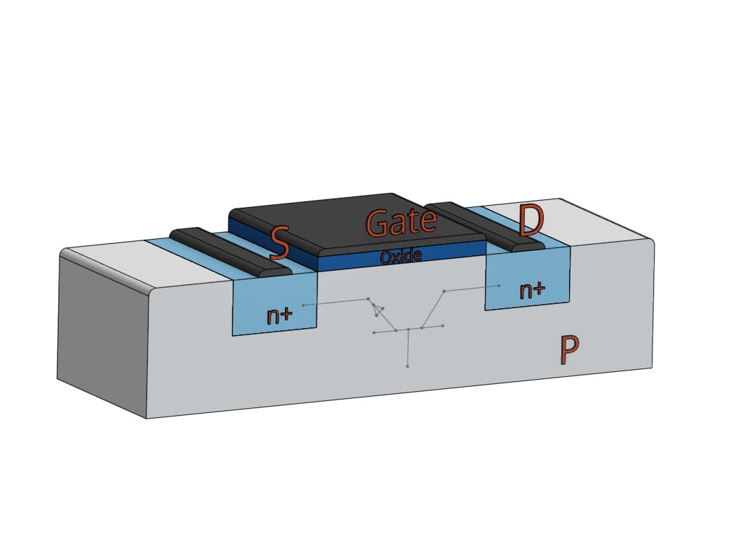
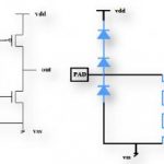
Lurking inside of every Mosfet is a parasitic bipolar junction transistor (BJT). Of course, in normal circuit operation the BJT does not play a role in the device operation. Accordingly, SPICE models for Mosfets do not behave well when the BJT is triggered. However, these models work just fine for most purposes. The one important… Read More
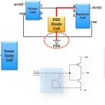
Terms like avalanche breakdown and impact ionization sound like they come from the world of science fiction. They do indeed come from a high stakes world, but one that plays out over and over again here and now, on a microscopic scale in semiconductor devices – namely as part of electrostatic discharge (ESD) protection. Semiconductor… Read More
Looking back, 2015 was a significant year for mergers and acquisitions in the EDA industry. The Semiwiki team maintains a chronology of major transactions here.
As I was reviewing this compendium, one of the entries that stands out is the acquisition of Apache Design Solutions by Ansys, Inc. a couple of years ago.
At that time, there… Read More
By Hend Wagieh, Mentor Graphics
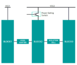
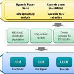
At advanced IC technology nodes, circuit designers are now encountering problems such as reduced voltage supply headroom, increased wiring parasitic resistance (Rp) and capacitance (Cp), more restrictive electromigration (EM) rules, latch-up, and electrostatic discharge (ESD) damage,… Read More
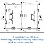
ESD has historically been a big problem analyzed with ad-hoc approaches. As explained earlier, this is no longer an adequate way to plan nor signoff ESD protection.
Pathfinder is the first full-chip comprehensive ESD planning and verification solution. It is targeted to address limitations in today’s methodologies.… Read More
Introduction
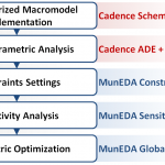
Circuit designers work at the transistor level and strive to get the ultimate in performance, layout density or low power by creating crafty circuit topologies in both schematics and layout. Along with this quest comes the daunting task of verifying that all of your rules and best practices about reliability have… Read More