
Introduction
Circuit designers work at the transistor level and strive to get the ultimate in performance, layout density or low power by creating crafty circuit topologies in both schematics and layout. Along with this quest comes the daunting task of verifying that all of your rules and best practices about reliability have been followed properly. While at Intel I debugged a DRAM design that had a yield loss issue caused by an electromigration failure, and this was at 6um design rules. We didn’t have any automated tools at that time to pinpoint where current density rules were exceeded. It simply meant that we created silicon, tested it, found reliability issues, fixed the issues, and re-spun another batch of silicon. This cost us valuable time to market delays.Lets take a quick look at several classes of circuits that would benefit from an Electrical Rule Checker (ERC) tool.
ESD Protection
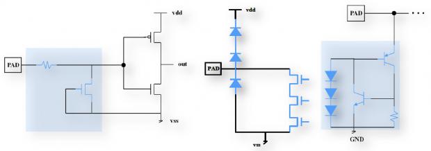
Consider what happens at the inputs and outputs for each pad in your IC design for ESD (Electro Static Discharge) protection.

On the left we have an input pad with clamp cell, and in the middle an output pad with diode protection for overshoot and undershoot. For the input pad layout there are special rules for the current densities allowed in creating the series resistor as shown in the following diagram:
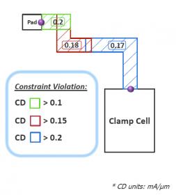
An ERC tool would need to read both the schematic and layout topologies, find the path from input pad to clamp cell, calculate current density along that path, compare current density versus the technology-specific constraints, and finally report any violations.A domain expert in ESD best practices should be able to program an ERC tool in order to automate the verification process.
Calibre PERC
Matthew Hogan is the TME at Mentor for their tool called Calibre PERC (Programmable Electrical Rule Checker) and he gave me an overview and demo last month. This tool automates the verification of transistor-level best practices in order to ensure first silicon success.
Multi-Power Domains
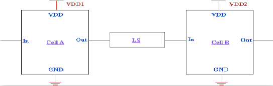
Portable consumer electronics like Smart Phones and Tablets are driving a large part of the semiconductor economy these days so it is import to have long battery life. This challenge is met by using a multi-power domain methodology where high speed sections have a higher power supply value than lower speed sections. Where these two power domains meet you need to insert a level shifter. PERC can verify if level shifters are in place.
Bulk Pin Connection
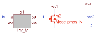
If your low-voltage PMOS device has the bulk connected to the wrong VCC supply it will function but also cause a reliability issue. With PERC you can write a rule to check for this condition:
Layout Based Verification
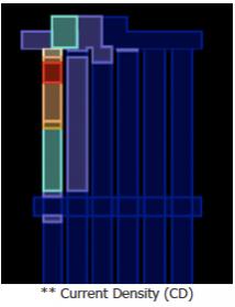
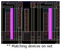
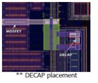
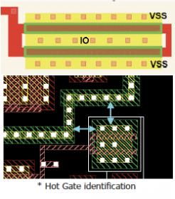
Rules can be described to find and report many classes important to reliability: Point to point resistance, current density, matching devices on a net, coupling de-cap placement, and hot gate identification.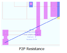
Visualization
During the demo I saw the syntax for PERC rules and what happened when these rules were run on a test schematic and layout.
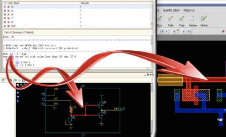
Each violation of a rule is highlighted, when I click a violation then I see both the schematic and layout windows appear and the violation is shown in red.
PDK
I think that the foundries will love this tool and should put in some effort to create and support PERC rules as part of their PDK (Process Design Kits). It’s really in their best interest to ensure first silicon success.
Conclusion
The Calibre PERC tool from Mentor combines ERC for both schematic and layout topologies so that you can enforce your own best practices across an IC design. Circuit designers can now use this methodology to check their designs for many classes (ESD, multi-power domain, AMS, etc.) of their circuits.


Comments
0 Replies to “Transistor-Level Electrical Rule Checking”
You must register or log in to view/post comments.