
By Hend Wagieh, Mentor Graphics
At advanced IC technology nodes, circuit designers are now encountering problems such as reduced voltage supply headroom, increased wiring parasitic resistance (Rp) and capacitance (Cp), more restrictive electromigration (EM) rules, latch-up, and electrostatic discharge (ESD) damage, which are all sources of possible circuit failure. While none of these effects suddenly appeared in the nanoscale era (sub-130nm), they have become progressively more serious, and must now be addressed during circuit verification to ensure robust designs and reliable operation.
ESD protection is one of the most important reliability issues in today’s CMOS integrated circuit (IC) products. ESD failures caused by thermal breakdown due to high current transient, or dielectric breakdown in gate oxide due to high voltage overstress, can result in either immediate failure of IC chips, or gradual degradation of circuit performance. To obtain high ESD resistance, CMOS ICs must be designed with on-chip ESD protection circuits at the input/output (I/O) pins and across the power lines. Turn-on-efficient ESD protection circuits clamp the overstress voltage across the gate oxide to limit the voltage swing.
The conventional approach to checking such circuitry is to use DRC rules to target areas of a layout that have potential reliability issues to check, which requires adding extra layers called “marker layers” to the IC layout database. Adding marker layers is a manual process, making it ripe for mistakes, and requires additional DRC runs, which extends verification time.
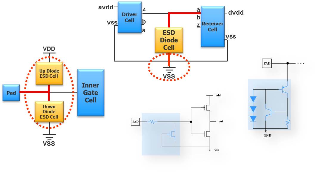
A better solution is provided by a circuit verification tool that automatically identifies the reliability-sensitive geometries and applies specialized physical checks to catch real design problems that impact circuit reliability. The Calibre® PERC™ tool uses information from an IC’s netlist to identify circuit topologies of interest, such as possible ESD paths and probable electrical failure sources, as well as the presence or absence of ESD protection circuits. For example, protection circuits are identified by recognizing device types and connectivity patterns based on any of the ESD configurations commonly known and widely used in designs today (Figure 1). Beyond verifying that the required circuits are present and connected properly, Calibre PERC measures the layout to ensure that interconnects are sufficiently sized to meet a maximum current density requirement. This can be accomplished without the need for marker layers or other manual interventions.

The ESD EDA working group has defined and recommended 39 ESD checks that can be implemented using Calibre PERC to assure a reliable design that is robust against ESD events and electrical failure. In these checks, ESD verification is performed on multiple levels, from cell level to package level, including intra-and inter-power domain ESD checks.
As an example, to implement verification of ESD protection between I/O and power rails, the tool performs the following steps:
[LIST=1]
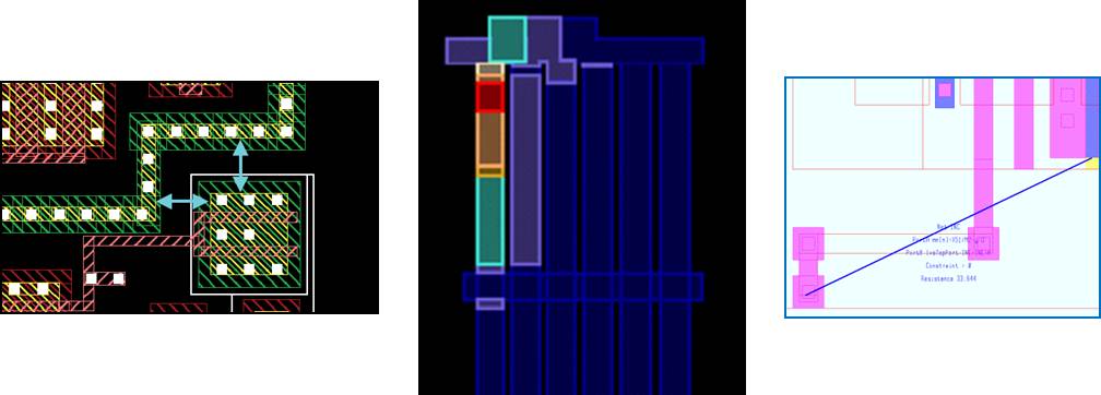
Since the tool is programmable, ESD checks can easily be expanded to cover parasitic extraction on metal interconnects, and design rule checks on selected ESD topologies, protected circuits, or violating circuits. It can also validate electrical compliance by performing resistance and current density analysis to ensure that the wiring of these devices is robust enough to support the largest currents that can be induced (Figure 2).
Automatic voltage propagation of input sources through the design, and voltage-dependent DRC checks, provide additional capabilities to simplify complex circuit verification. For example, the tool can be used to perform advanced electrical rule checks (AERC), which identifies signal lines crossing voltage domains in mixed-signal or multi-domain low power digital designs.
Additional information about advanced ESD checking can be found in the white paper entitled Solving Electrostatic Discharge Design Issues with Calibre PERC.
Hend Wagieh is a Senior Technical Marketing Engineer for Calibre Design Solutions at Mentor Graphics. She may be contacted at hend_wagieh@mentor.com.
Share this post via:


Comments
2 Replies to “Automating Complex Circuit Checking Tasks”
You must register or log in to view/post comments.