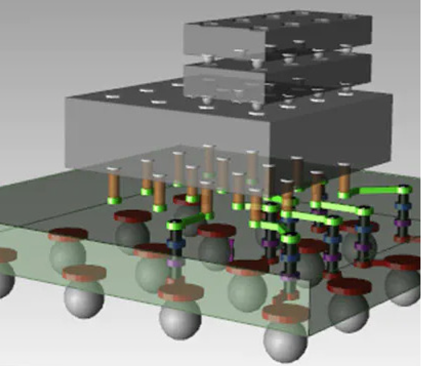
One of the most promising advancements in the semiconductor field is the development of 3D Integrated Circuits (3D ICs). 3D ICs enable companies to partition semiconductor designs and seamlessly integrate silicon Intellectual Property (IP) at the most suitable process nodes and processes. This strategic partitioning yields an array of benefits, including reduced latency, high-bandwidth data transfer, lower manufacturing costs, increased wafer yields, minimized power consumption, and ultimately, lower overall costs. While not yet mainstream, the growing standardization of chiplets and the development of supporting tools are paving the way for the practical and profitable implementation of 3D ICs for both large and small players. These appealing benefits have driven significant growth and development in advanced heterogeneous packaging and 3D IC technology. However, this progress has also introduced challenges related to manufacturability and reliability and must be addressed for 3D ICs to become a mainstream reality.
Siemens EDA has published an eBook that addresses these challenges and offers up solutions to help deliver 3D IC semiconductor reliability. Anyone involved in the development of 3D ICs will find the eBook very informative. The following is an overview of the salient points from the book.
Challenges in Ensuring 3D IC Semiconductor Reliability
3D ICs have brought with them a host of challenges, spanning the selection of tools and methodologies, parasitic extraction, and the task of heterogeneous integration.

Sign-off strategies of 2D ICs heavily rely on design rule kits provided by foundries, typically designed for single-process System-on-Chip (SoC) designs. However, this conventional approach falls short in the realm of 3D IC advanced heterogeneous packaging, where multiple layers with varying processes are involved. Traditional LVS relies on recognizing electrical connections between pins, a feature that passive components lack by definition. To address this, a method is required to comprehend the impact of passive components and consider their interconnection role alongside active devices. This is critical as accurate post-assembly netlisting and simulation results hinge on detailed wire placements and material information. Unlike System-on-Chips (SoCs) that are coplanar, 3D ICs incorporate stacking with components at different vertical depths, rendering them non-coplanar. This non-coplanar nature introduces intricate challenges for semiconductor and IC packaging designers, particularly regarding the assessment of interactions between components with different process technologies and iterative evaluations. The issue also involves determining which interactions are essential to verify to avoid wasting resources on unnecessary checks, further complicating the design and manufacturing process of 3D ICs.
Solutions for 3D IC Semiconductor Reliability
Overcoming these challenges necessitates a blend of innovative strategies, tools, and methodologies.
Accurate Modeling: The initial step in addressing the challenges of 3D ICs is the creation of highly accurate models. Components like Through-Silicon Vias (TSVs) require precise modeling to account for their parasitic elements.
Parasitic Extraction: Accurate parasitic extraction is vital for understanding the effects of these new components on signal integrity, power efficiency, and overall performance. Utilizing advanced extraction tools enables engineers to capture intricate parasitic elements introduced by components like TSVs and micro bumps.
Data Representation: For organic-based (PCB-oriented) 3D ICs, intelligent data representation is paramount. This entails including information such as net names, via details, and structural elements natively in the design database, streamlining the setup time for parasitic extractions and reducing the likelihood of errors.
Early Planning and Floorplanning: The utilization of planning tools is critical to facilitate the integration of diverse components and the creation of a reliable floorplan. This planning step is indispensable for comprehending the interactions between different layers and components within a 3D IC.
Summary
The challenges in ensuring the reliability of 3D ICs are considerable. However, by embracing innovative tools, methodologies, and intelligent data representation, it’s feasible to overcome these hurdles. With accurate modeling, precise parasitic extraction, and innovative design strategies, engineers can unlock the full potential of 3D IC technology while adhering to the highest standards of reliability. As the semiconductor industry evolves, 3D ICs are set to play a pivotal role in shaping the future of electronic devices, promising more powerful, energy-efficient, and compact solutions for consumers.
Also Read:
The Path to Chiplet Architecture
AI for the design of Custom, Analog Mixed-Signal ICs
Share this post via:


Comments
There are no comments yet.
You must register or log in to view/post comments.