You are currently viewing SemiWiki as a guest which gives you limited access to the site. To view blog comments and experience other SemiWiki features you must be a registered member. Registration is fast, simple, and absolutely free so please,
join our community today!
In the rapidly evolving landscape of semiconductor manufacturing, the demand for processors that handle increasing workloads while maintaining power efficiency and compact form factors has never been higher. Intel’s Foveros 2.5D packaging technology emerges as a pivotal innovation, enabling denser die integration… Read More
The semiconductor industry is facing a paradigm shift. Traditional scaling, once driven by Moore’s Law, is slowing down. For years, moving to smaller process nodes led to lower transistor costs and better performance. However, scaling from node to node now offers fewer benefits as wafer costs rise much more than the historical… Read More
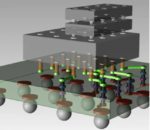
One of the most promising advancements in the semiconductor field is the development of 3D Integrated Circuits (3D ICs). 3D ICs enable companies to partition semiconductor designs and seamlessly integrate silicon Intellectual Property (IP) at the most suitable process nodes and processes. This strategic partitioning yields… Read More
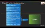
As I have been watching the developments in EDA and Semiconductor industry, it is apparent that we remain fragmented unless pushed to adopt a common standard mostly due to business reasons. Foundries are dictating on the rules to be followed by designs, thereby EDA tools incorporating them. Also, design companies needed to work… Read More
Testing, testing… 3D ICsby Beth Martin on 10-06-2011 at 7:01 pmCategories: EDA, Siemens EDA
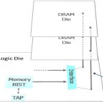
3D ICs complicate silicon testing, but solutions exist now to many of the key challenges. – by Stephen Pateras
The next phase of semiconductor designs will see the adoption of 3D IC packages, vertical stacks of multiple bare die connected directly though the silicon. Through-silicon vias (TSV) result in shorter and thinner… Read More