You are currently viewing SemiWiki as a guest which gives you limited access to the site. To view blog comments and experience other SemiWiki features you must be a registered member. Registration is fast, simple, and absolutely free so please,
join our community today!
            WP_Term Object
(
    [term_id] => 24
    [name] => TSMC
    [slug] => tsmc
    [term_group] => 0
    [term_taxonomy_id] => 24
    [taxonomy] => category
    [description] =>
    [parent] => 158
    [count] => 621
    [filter] => raw
    [cat_ID] => 24
    [category_count] => 621
    [category_description] =>
    [cat_name] => TSMC
    [category_nicename] => tsmc
    [category_parent] => 158
    [is_post] =>
)

WP_Term Object
(
    [term_id] => 24
    [name] => TSMC
    [slug] => tsmc
    [term_group] => 0
    [term_taxonomy_id] => 24
    [taxonomy] => category
    [description] =>
    [parent] => 158
    [count] => 621
    [filter] => raw
    [cat_ID] => 24
    [category_count] => 621
    [category_description] =>
    [cat_name] => TSMC
    [category_nicename] => tsmc
    [category_parent] => 158
    [is_post] =>
)
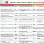
The TSMC OIP DAC Theater schedule is finalized and ready to go. It kicks off Monday at 10:15 am in booth #1629 and ends with a raffle at 5:45 pm each day (Mon-Tue-Wed) TSMC gives out some very nice prizes so check in with the TSMC booth staff when you arrive. There are 66 coveted presentation spots representing the top ecosystem partners… Read More
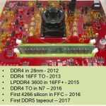
Will we see DDR5 memory (device) and memory controller (IP) in the near future? According with Cadence who has released the first test chip in the industry integrating DDR5 memory controller IP, fabricated in TSMC’s 7nm process and achieving a 4400 megatransfers per second (MT/sec) data rate, the answer is clearly YES !
Let’s come… Read More
At TSMC 2018 Silcon Valley Technology Symposium, Dr Kevin Zhang, TSMC VP of Business Development covered technology updates for IoT platform. The three growth drivers in this segment namely TSMC low power, RF enhancement and embedded memory technology (MRAM/RRAM) reinforced both progress and growth in global semiconductor… Read More
During TSMC 2018 Technology Symposium, Dr. B.J. Woo, TSMC VP of Business Development presented market trends in the area of mobile applications and HPC computing as well as shared TSMC progress in making breakthrough efforts in the technology offerings to serve these two market segments.
Both 5G and AI are taking the center stage… Read More
Here are the Top 10 highlights from the recent TSMC 2018 Technology Symposium, held in Santa Clara CA. A couple of years ago, TSMC acknowledged the unique requirements of 4 different market segments, which has since guided their process development strategy — Mobile, High-Performance Computing (HPC), Automotive, and… Read More
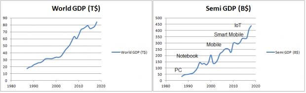
The most viewed blogs I write for SemiWiki are consistently blogs comparing the four leading edge logic producers, GLOBALFOUNDRIES (GF), Intel, Samsung (SS) and TSMC. Since the last time I compared the leading edge new data has become available and several new processes have been introduced. In this blog I will update the current… Read More
In case you missed the TSMC event, ANSYS and TSMC are going to reprise a very important topic – signing-off reliability for ADAS and semi-autonomous /autonomous systems. This topic hasn’t had a lot of media attention amid the glamor and glitz of what might be possible in driverless cars. But it now seems like the cold light of real … Read More
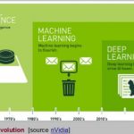
How could we differentiate between deep learning and machine learning as there are many ways of describing them? A simple definition of these software terms can be found here. Let’s look into Artificial Intelligence (AI), which was coined back in 1956. The term AI can be defined as human intelligence exhibited by machines.… Read More
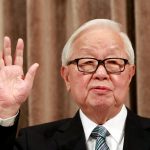
The TSMC Q4 2017 earnings call transcript is up and I found it to be quite interesting for several reasons. First and foremost, this is the last call Chairman Dr. Morris Chang will participate in which signifies the end of a world changing era for me and the fabless semiconductor ecosystem, absolutely. TSMC announced his retirement… Read More
I was invited to give a talk at the ISS conference on the Impact of EUV on the Semiconductor Supply Chain. The ISS conference is an annual gathering of semiconductor executives to review technology and global trends. In this article I will walk through my presentation and conclusions.… Read More