You are currently viewing SemiWiki as a guest which gives you limited access to the site. To view blog comments and experience other SemiWiki features you must be a registered member. Registration is fast, simple, and absolutely free so please,
join our community today!
            WP_Term Object
(
    [term_id] => 24
    [name] => TSMC
    [slug] => tsmc
    [term_group] => 0
    [term_taxonomy_id] => 24
    [taxonomy] => category
    [description] =>
    [parent] => 158
    [count] => 647
    [filter] => raw
    [cat_ID] => 24
    [category_count] => 647
    [category_description] =>
    [cat_name] => TSMC
    [category_nicename] => tsmc
    [category_parent] => 158
    [is_post] =>
)

WP_Term Object
(
    [term_id] => 24
    [name] => TSMC
    [slug] => tsmc
    [term_group] => 0
    [term_taxonomy_id] => 24
    [taxonomy] => category
    [description] =>
    [parent] => 158
    [count] => 647
    [filter] => raw
    [cat_ID] => 24
    [category_count] => 647
    [category_description] =>
    [cat_name] => TSMC
    [category_nicename] => tsmc
    [category_parent] => 158
    [is_post] =>
)
The EUV Divide
I was recently updating an analysis I did last year that looked at EUV system supply and demand, while doing this I started thinking about Intel and their Fab portfolio.
If you look at Intel’s history as a microprocessor manufacturer, they are typically ramping up their newest process node (n), in volume production… Read More
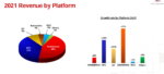
Hello! The most important semiconductor company in the world reported earnings last night. It’s been something of a tradition to post Taiwan Semiconductor Company (TSMC) earnings posts not behind my paywall, and I think that I’m going to continue that to kickoff each earnings season.
There are so many threads in the TSMC call that… Read More
The further scaling of interconnect and via lithography for advanced nodes is challenged by the requirement to provide a process window that supports post-patterning critical dimension variations and mask overlay tolerances. At the recent international Electron Devices Meeting (IEDM) in San Francisco, TSMC presented … Read More
Previous SemiWiki articles have described the evolution of embedded non-volatile memory (eNVM) IP from (charge-based) eFlash technology to alternative (resistive) bitcell devices. (link, link)
The applications for eNVM are vast, and growing. For example, microcontrollers (MCUs) integrate non-volatile memory for … Read More
Advanced 2.5D/3D Packaging Roadmapby Tom Dillinger on 01-03-2022 at 6:00 amCategories: Events, Semiconductor, TSMC
Frequent SemiWiki readers are no doubt familiar with the advances in packaging technology introduced over the past decade. At the recent International Electron Devices Meeting (IEDM) in San Francisco, TSMC gave an insightful presentation sharing their vision for packaging roadmap goals and challenges, to address the growing… Read More
TSMC drew the ire of Chinese state media last week after it complied with the US Department of Commerce request to submit supply chain data by the November 8 deadline.
The Chinese reports, which called it an act of “surrender” to US hegemony, were careful in laying blame on Taipei for caving in to Washington, rather than pointing fingers… Read More
This is an interesting piece of TSMC history. From 1987 to 1988 James E. Dykes served as the first President and Chief Executive Officer of Taiwan Semiconductor Manufacturing Company Ltd.
Taiwan Semiconductor Outlook
by James E. Dykes
President & Chief Executive Officer
Taiwan Semiconductor Manufacturing Company
Given… Read More
TSMC recently held their 10th annual Open Innovation Platform (OIP) Ecosystem Forum. An earlier article summarized the highlights of the keynote presentation from L.C. Lu, TSMC Fellow and Vice-President, Design and Technology Platform, entitled “TSMC and Its Ecosystem for Innovation” (link).
Overview of 3D Fabric
The TSMC… Read More
TSMC recently held their Open Innovation Platform (OIP) Ecosystem Forum event where many of their key partners presented on their latest projects and developments. This year one of their top IP provider partners, Analog Bits, gave two presentations. Analog building blocks have always been necessary as enabling technology … Read More
TSMC recently held their 10th annual Open Innovation Platform (OIP) Ecosystem Forum. An earlier article summarized the highlights of the keynote presentation from L.C. Lu, TSMC Fellow and Vice-President, Design and Technology Platform, entitled “TSMC and Its Ecosystem for Innovation” (link).
One of the topics that L.C. … Read More