You are currently viewing SemiWiki as a guest which gives you limited access to the site. To view blog comments and experience other SemiWiki features you must be a registered member. Registration is fast, simple, and absolutely free so please,
join our community today!
            WP_Term Object
(
    [term_id] => 24
    [name] => TSMC
    [slug] => tsmc
    [term_group] => 0
    [term_taxonomy_id] => 24
    [taxonomy] => category
    [description] =>
    [parent] => 158
    [count] => 642
    [filter] => raw
    [cat_ID] => 24
    [category_count] => 642
    [category_description] =>
    [cat_name] => TSMC
    [category_nicename] => tsmc
    [category_parent] => 158
    [is_post] =>
)

WP_Term Object
(
    [term_id] => 24
    [name] => TSMC
    [slug] => tsmc
    [term_group] => 0
    [term_taxonomy_id] => 24
    [taxonomy] => category
    [description] =>
    [parent] => 158
    [count] => 642
    [filter] => raw
    [cat_ID] => 24
    [category_count] => 642
    [category_description] =>
    [cat_name] => TSMC
    [category_nicename] => tsmc
    [category_parent] => 158
    [is_post] =>
)
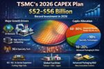
The opening of the TSMC 2026 earning call series brought no surprises. CC Wei has done more than 30 such calls since taking the CEO position in 2018 and he never fails to disappoint. Once again, CC Wei reported numbers above guidance driven by strong demand and flawless execution. This illustrates the benefit of TSMC’s close collaborations… Read More
One of my favorite times of the year is coming (sailing season) and my favorite event of the year is coming as the company I most respect will host the best international semiconductor networking event starting here in Silicon Valley.
The 32nd annual TSMC Technology Symposium represents one of the most influential events in the … Read More
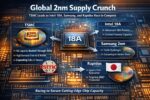
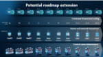
The semiconductor industry is in the midst of a structural supply challenge that’s tightly coupled to exploding demand for advanced chips, especially those used in AI, HPC, and next-generation mobile and consumer devices. At the center of this vortex is the 2nm class of manufacturing technology, representing one of the most … Read More
In the modern world, the semiconductor industry stands at the heart of technological innovation. From smartphones and laptops to advanced medical devices and artificial intelligence systems, nearly every piece of contemporary electronics depends on increasingly sophisticated microchips. Among the leading companies … Read More
TSMC continues to reinforce its leadership in advanced semiconductor manufacturing through its deepening collaboration with Cadence Design Systems. The expanded partnership focuses on enabling next-generation artificial intelligence and high-performance computing innovations by aligning advanced electronic design… Read More
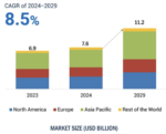
The global semiconductor industry sits at the foundation of modern technology, powering everything from smartphones and cloud data centers to artificial intelligence, automobiles, and national defense systems. At the center of advanced chip manufacturing are three major players: TSMC, Samsung Foundry, and Intel Foundry… Read More
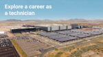
The expansion of semiconductor manufacturing in the United States, particularly with TSMC’s multi-fab campus in Phoenix, Arizona, has created a significant need for skilled technical workers. To meet this demand, TSMC has partnered with educational institutions, including Grand Canyon University (GCU), to launch… Read More
NanoIC has announced a major expansion of its process design kit portfolio with the introduction of its first A14 logic and embedded eDRAM memory PDK. This milestone reflects the company’s growing role in enabling advanced semiconductor design at cutting-edge technology nodes and addresses increasing industry demand for… Read More
In February of 2026, Taiwan Semiconductor Manufacturing Company (TSMC) will host the TSMC AZ Exclusive Experience Day in Phoenix, Arizona, offering selected participants a rare opportunity to engage directly with one of the most advanced semiconductor manufacturing organizations in the world. The event will serve as an immersive… Read More
When Morris Chang left Texas Instruments in 1983 to found TSMC, he was not merely starting a new company—he was proposing a new industrial logic. Chang recognized that semiconductor manufacturing had become so capital-intensive that it could no longer survive as just one function inside a vertically integrated company.… Read More