You are currently viewing SemiWiki as a guest which gives you limited access to the site. To view blog comments and experience other SemiWiki features you must be a registered member. Registration is fast, simple, and absolutely free so please,
join our community today!
            WP_Term Object
(
    [term_id] => 24
    [name] => TSMC
    [slug] => tsmc
    [term_group] => 0
    [term_taxonomy_id] => 24
    [taxonomy] => category
    [description] =>
    [parent] => 158
    [count] => 621
    [filter] => raw
    [cat_ID] => 24
    [category_count] => 621
    [category_description] =>
    [cat_name] => TSMC
    [category_nicename] => tsmc
    [category_parent] => 158
    [is_post] =>
)

WP_Term Object
(
    [term_id] => 24
    [name] => TSMC
    [slug] => tsmc
    [term_group] => 0
    [term_taxonomy_id] => 24
    [taxonomy] => category
    [description] =>
    [parent] => 158
    [count] => 621
    [filter] => raw
    [cat_ID] => 24
    [category_count] => 621
    [category_description] =>
    [cat_name] => TSMC
    [category_nicename] => tsmc
    [category_parent] => 158
    [is_post] =>
)
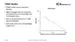
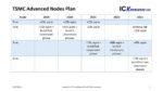
The TSMC Symposium kicked of today. I will share my general thoughts while Tom Dillinger will do deep dives on the technology side. The event started with a keynote by TSMC CEO CC Wei followed by technology presentations by the TSMC executive staff.
C.C. Wei introduced a new sound bite this year that really resonated with me and that… Read More
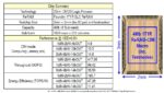
IBM has announced the development of a 2nm process.
IBM Announcement
What was announced:
- “2nm”
- 50 billion transistors in a “thumbnail” sized area later disclosed to be 150mm2 = 333 million transistors per millimeter (MTx/mm2).
- 44nm Contacted Poly Pitch (CPP) with 12nm gate length.
- Gate All Around (GAA), there are several ways
…
Read More
-Chip shortage on 60 Minutes- Average Joe now aware of chip issue
-Intel sprinkling fairy dust (money) on New Mexico & Israel
-Give up on buy backs and dividends
-Could Uncle Sam give a handout to Intel?
You normally don’t want to answer the door if 60 Minutes TV crew is outside as it likely doesn’t mean good things.… Read More
TSMC recently announced plans to spend $100 billion dollars over three years on capital. For 2021 they announced $30B in total capital with 80% on advanced nodes (7nm and smaller), 10% on packaging and masks and 10% on “specialty”.
If we take a guess at the capital for each year, we can project something like $30B for 2021 (announced),… Read More
We were all pleasantly surprised when TSMC increased 2021 Capex to a record $28 billion. To me this validated the talk inside the ecosystem that Intel would be coming to TSMC at 3nm. We were again surprised when TSMC announced a $100B investment over the next three years which belittled Intel’s announcement that they would spend … Read More
– Intel announced 2 new fabs & New Foundry Services
– Not only do they want to catch TSMC they want to beat them
– It’s a very, very tall order for a company that hasn’t executed
– It will require more than a makeover to get to IDM 2.0
Intel not only wants to catch TSMC but beat them at their own … Read More
The term von Neumann bottleneck is used to denote the issue with the efficiency of the architecture that separates computational resources from data memory. The transfer of data from memory to the CPU contributes substantially to the latency, and dissipates a significant percentage of the overall energy associated with … Read More
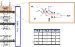
All-Digital In-Memory Computingby Tom Dillinger on 03-15-2021 at 6:00 amCategories: Events, Foundries, TSMC
Research pursuing in-memory computing architectures is extremely active. At the recent International Solid State Circuits conference (ISSCC 2021), multiple technical sessions were dedicated to novel memory array technologies to support the computational demand of machine learning algorithms.
The inefficiencies associated… Read More
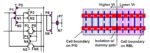
Register File Design at the 5nm Nodeby Tom Dillinger on 03-10-2021 at 2:00 pmCategories: Events, Foundries, TSMC
“What are the tradeoffs when designing a register file?” Engineering graduates pursuing a career in microelectronics might expect to be asked this question during a job interview. (I was.)
On the surface, one might reply, “Well, a register file is just like any other memory array – address inputs, data inputs and outputs, read/write… Read More
There are reports in the media that TSMC is now planning six Fabs in Arizona (the image above is Fab 18 in Taiwan). The original post I saw referred to a Megafab and claimed six fabs with 100,000 wafers per month of capacity (wpm) for $35 billion dollars. The report further claimed it would be larger than TSMC fabs in Taiwan.
This report… Read More