Just at the moment we look for the mobile market to consolidate, it fractures along new fault lines as old allies become enemies and new business models appear in order to spur the ecosystem giants forward. It was not long ago that Android was let loose in an attempt to prove that the Mobile World is Flat. Ah but Samsung decided that it… Read More
Meeting with Sidense at TSMC Technology Symposium
If you have attended DAC in Austin (June 2-5), you probably have missed the first TSMC Technology Symposium. It was held on June 6 in Shanghai. Considering my own experience of a 29 hours trip to come back home (in France), I doubt that it was any possible to leave Austin on June 5 to attend TSMC Technology Symposium in Shanghai on June… Read More
…And Now Intel Will Make a Turn Towards Memories as it Plans to Capture Samsung
While eyes remain fixated on the architectural battle between Intel and ARM, a second front is soon about to open up that will determine mobile supremacy for the rest of the decade. Whereas yesterday’s story on the collapse of Wintel and the anointing of Google and Samsung are repeated endlessly, now tables are being set for a significant… Read More
The Return of the "Moore Noyce" Company
It has been a little over a fortnight since Paul Otellini officially stepped down from the CEO post and yet it seems to be more than a long time gone. Unlike his predecessors, he was not asked to remain on the board and perhaps it is a sign that his complete disengagement from the company was necessary to complete a future strategic engagement.… Read More
Enabling 14nm FinFET Design
There’s never a dull moment in the foundry race to offer FinFET processes that enable leading-edge SoC design. Today I attended a webinar hosted by Samsung and Synopsys on how to enable 14nm FinFET design. The two speakers were Dr. Kuang-Kuo Lin from Samsung and Dr. Henry Sheng from Synopsys.
Dr. Kuang-Kuo Lin, Samsung
Dr.… Read More
TSMC Goes To DAC
TSMC will be at DAC again this year, of course. The main event, as last year, is the OIP Theater where TSMC’s partners come and present their collaboration stories. Here is the schedule:… Read More
The Morphing of Intel’s Monopoly
It was a generation ago when Intel, less than three years old, created the three fundamental building blocks of the compute era: the DRAM, the EPROM and the Microprocessor, an incredible feat of innovation by any measure. Manufacturing yield, not power or performance determined success of failure and in the first two … Read More
IP Quality: Foundation of a Successful Ecosystem
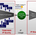
Talking about Design IP (I mean successful Design IP) lead you to quickly pronounce the two magic key words: Quality and Ecosystem. Those who remember the IP emergence in the mid 90’s know very well why Quality has to be a prerequisite when dealing with Design IP, as they probably have paid the price of mediocre IP quality at that time.… Read More
How To Design a TSMC 20nm Chip with Cadence Tools
Every process node these days has a new “gotcha” that designers need to be aware of. In some ways this has always been the case but the changes used to be gradual. But now each process node has something discontinuously different. At 20nm the big change is double patterning. At 14/16nm it is FinFET.
Rahul Deokar and John… Read More
Global Foundries Does DAC
Global Foundries will be at DAC in booth 1314. There will be 6 pods there demonstrating:
- Advanced Technology: 28nm ready and ramping, and next is 20LPM and 14XM.
- PDKs: For 28nm, 20nm and 14nm. 14nm handles FinFET enablement complexity. Robust, easy to use and high quality, supports pretty much the full range of EDA tools.
- Design


The Semiconductor Growth Numbers are Insane but the Real World Doesn’t Tally!