You are currently viewing SemiWiki as a guest which gives you limited access to the site. To view blog comments and experience other SemiWiki features you must be a registered member. Registration is fast, simple, and absolutely free so please,
join our community today!
WP_Term Object
(
    [term_id] => 16126
    [name] => Lithography
    [slug] => lithography
    [term_group] => 0
    [term_taxonomy_id] => 16126
    [taxonomy] => category
    [description] =>
    [parent] => 0
    [count] => 189
    [filter] => raw
    [cat_ID] => 16126
    [category_count] => 189
    [category_description] =>
    [cat_name] => Lithography
    [category_nicename] => lithography
    [category_parent] => 0
    [is_post] =>
)
There is growing awareness that EUV lithography is actually an imaging technique that heavily depends on the distribution of secondary electrons in the resist layer [1-5]. The stochastic aspects should be traced not only to the discrete number of photons absorbed but also the electrons that are subsequently released. The electron… Read More
The 3nm node is projected to feature around a 22 nm metal pitch [1,2]. This poses some new challenges for the use of EUV lithography. Some challenges are different for the 0.33NA vs. 0.55NA systems.
0.33 NA
For 0.33 NA systems, 22 nm pitch can only be supported by illumination filling 4% of the pupil, well below the 20% lower limit for
…
Read More
-If you can’t beat them, embargo them
-It has been reported US wants ASML to halt China DUV tools
-US obviously wants to kill, not just wound China chip biz
-Is this embargo the alternative to failed CHIPS act?
-Hard to say “do as I say, not as I do”- but US does anyway
First EUV ban now DUV ban? Are process & yield… Read More
At the 2022 SPIE Advanced Lithography Conference, ASML presented an update on EUV. I recently had a chance to go over the presentations with Mike Lercel of ASML. The following is a summary of our discussions.
0.33 NA
The 0.33 NA EUV systems are the production workhorse systems for leading edge lithography today. 0.33 NA systems are… Read More
The next generation of EUV lithography systems are based on a numerical aperture (NA) of 0.55, a 67% increase from the current value of 0.33. It targets being able to print 16 nm pitch [1]. The High-NA systems are already expected to face complications from four issues: (1) reduced depth-of-focus requires thinner resists, which… Read More
To the general public, EUV lithography’s resolution can be traced back to its short wavelengths (13.2-13.8 nm), but the true printed resolution has always been affected by the stochastic behavior of the electrons released by EUV absorption [1-5].
A 0.33 NA EUV system is expected to have a diffraction-limited point spread… Read More
At this year’s SPIE Advanced Lithography conference, changes to EUV masks were particularly highlighted, as a better understanding of their behavior is becoming clear. It’s now confirmed that a seemingly symmetric EUV mask absorber pattern does not produce a symmetric image at the wafer, as a conventional DUV … Read More
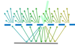
As a consequence of having a ~13.5 nm wavelength, EUV photons transfer ~90% of their energy to ionized photoelectrons. Thus, EUV lithography is fundamentally mostly EUV photoelectron lithography. The actual resolution becomes dependent on photoelectron trajectories.
Photoelectron trajectories in EUV lithography were… Read More
The list of possible stochastic patterning issues for EUV lithography keeps growing longer: CD variation, edge roughness, placement error, defects [1]. The origins of stochastic behavior are now well-known. For a given EUV photon flux into the resist, a limited fraction are absorbed. Since the absorption is less than 5% affected… Read More
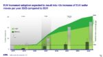
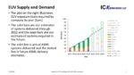
In my “The EUV Divide and Intel Foundry Services” article available here, I discussed the looming EUV shortage. Two days ago, Intel announced their first EUV tool installed at their new Fab 34 in Ireland is a tool they moved from Oregon. This is another indication of the scarcity of EUV tools.
I have been tracking EUV system production… Read More


ASML High-NA EUV is Not Ready for High-Volume Production