You are currently viewing SemiWiki as a guest which gives you limited access to the site. To view blog comments and experience other SemiWiki features you must be a registered member. Registration is fast, simple, and absolutely free so please,
join our community today!
WP_Term Object
(
    [term_id] => 50
    [name] => Events
    [slug] => events
    [term_group] => 0
    [term_taxonomy_id] => 50
    [taxonomy] => category
    [description] =>
    [parent] => 0
    [count] => 1375
    [filter] => raw
    [cat_ID] => 50
    [category_count] => 1375
    [category_description] =>
    [cat_name] => Events
    [category_nicename] => events
    [category_parent] => 0
    [is_post] =>
)
Hardware is roaring back into prominence in technology innovation, from advanced cars to robots, smart homes and smart cities, 5G communication and the burgeoning electronification of industry, medicine and utilities. While software continues to play a role, all of these capabilities depend fundamentally on advances in … Read More
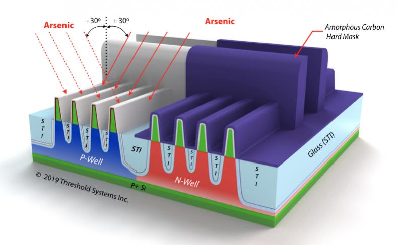
Part 4 of this series discussed how a transistor Extension could be fabricated in a planar device without using an implant operation, and is instead formed using a preferential etch followed by a selective epitaxial deposition. This final installment of the series will present the formation of an Extension in a FinFET transistor… Read More
Hello Cambridge, Grenoble, Stockholm, Moscow, Munich and Amsterdam
Our 2019 global symposiums and workshops have been hugely successful in promoting the RISC-V ISA and fostering expansive collaboration within the open-source community. It’s invigorating to see how the worldwide semiconductor ecosystem is energized and… Read More
Perhaps the most innovative and effective Extension implant does not involve an implant at all, but is instead an etch followed by a selective epitaxial deposition.
In this Extension fabrication methodology the Source/Drains regions in a planar device are etched away in the normal fashion to accommodate the replacement Source/Drain… Read More
Reason number ONE:The next five DACs will be in San Francisco and this will probably be the last one held in Las Vegas so you absolutely do NOT want to miss it. One of my most memorable DACs was in Las Vegas in 1985. My wife came with me for our second honeymoon and, by definition, it was just that, a honeymoon. This year we will probably spend… Read More
Just two more weeks before the 2019 CEO Outlook Thursday, May 23, at SEMI. If you haven’t registered yet, do so today. We’re expecting a full house as a result of our powerhouse lineup and networking opportunities.
That lineup includes Ed Sperling, editor in chief of Semiconductor Engineering, who will serve as moderator. Panelists… Read More
Anirudh Devgan (President of Cadence), gave the third keynote at CDNLive Silicon Valley this year. He has clearly become adept in this role. He has a big, but supportable vision for Cadence across markets and technologies and he’s become a master of the annual tech reveals that I usually associate with keynotes.
Anirudh opened … Read More
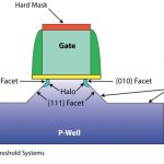
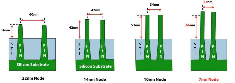
The problem of traditional FinFET Extension Implant doping concerns the awkward 3-dimensional structure of the fin. Because the Extension Implant defines the conductive electrical pathway between the Source/Drains and the undoped channel portion of the fin, it is essential that the fin be uniformly doped all three of its surfaces… Read More
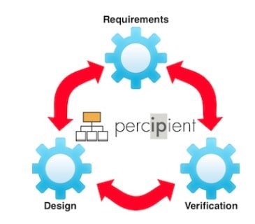
To me the major idea of ISO 26262 compliance is ensuring that requirements can be traced throughout the entire design and verification process, including the use of IP blocks. The first market application that comes to mind with ISO 26262 is automotive, with its emphasis on safety because human lives are at stake. Since necessity… Read More
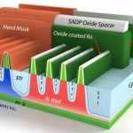
The use of hard masks instead of photoresist for the Extension implant is an effective way to optimize the amount of dopant that is retained along the fin sidewalls for those fins that border along photoresist edges (as discussed in Part 1 of this series).
However, hard masks do nothing to address the dominant problem driving steeper… Read More


Flynn Was Right: How a 2003 Warning Foretold Today’s Architectural Pivot