You are currently viewing SemiWiki as a guest which gives you limited access to the site. To view blog comments and experience other SemiWiki features you must be a registered member. Registration is fast, simple, and absolutely free so please,
join our community today!
WP_Term Object
(
    [term_id] => 50
    [name] => Events
    [slug] => events
    [term_group] => 0
    [term_taxonomy_id] => 50
    [taxonomy] => category
    [description] =>
    [parent] => 0
    [count] => 1374
    [filter] => raw
    [cat_ID] => 50
    [category_count] => 1374
    [category_description] =>
    [cat_name] => Events
    [category_nicename] => events
    [category_parent] => 0
    [is_post] =>
)
The commonly advanced reason for IP reuse is lower cost and shorter development time. However, IP reuse presents its own challenges, especially for analog designs. In the case of digital designs, once a new standard cell library is available, it is usually not too hard to resynthesize RTL to create new working silicon. For analog… Read More
I wasn’t able to attend the SPIE Advanced Lithography Conference this year for personal reasons, but Applied Materials was kind enough to set up a phone briefing for me with Regina Freed to discuss their Materials-Enabled Patterning announcement.
At IEDM Applied Materials (AMAT) tried to put together a panel across the entire… Read More
I had the opportunity to preview an upcoming webinar on SemiWiki that deals with design robustness for signoff regarding advanced node digital designs (think single-digit nanometers). “Design robustness” is a key term – it refers to high quality, high yielding SoCs that come up quickly and reliably in the target system. We all… Read More
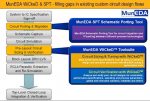
Before starting your next FPGA Prototyping Project you should catch the next SemiWiki webinar – “Six Automated Steps to Design Partitioning for Multi-FPGA Prototyping Boards”, in partnership with Aldec.
A significant portion of my 30+ years in the EDA industry has revolved around design verification with some form of FPGA … Read More
Technological leadership has long been key to TSMC’s success and they are following up their leadership development of 5nm with the world’s smallest SRAM cell at 0.021um 2 with circuit design details of their write assist techniques necessary to achieve the full potential of this revolutionary technology. In addition to their… Read More
At DesignCon 2020, there was a presentation by Micron, Socionext and Cadence that discussed design challenges and strategies for using the new low-power DDR specification (LPDDR5). As is the case with many presentations at DesignCon, ecosystem collaboration was emphasized. Justin Butterfield (senior engineer at Micron)… Read More
At DesignCon 2020, ANSYS held a series of sponsored presentations. I was able to attend a couple of them. These were excellent events with the material delivered by talented and high-energy speakers. The DesignCon technical program has many dimensions beyond the conference tracks. One of the presentations dealt with 3D ICs.… Read More
PowerMOS devices play a major role in a variety of power converter and control circuits. Some examples of their applications include PMICs, or boost and buck converters. Often these are used in mobile and IoT devices to convert battery voltages to circuit operating voltages.
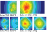
Due to their size and internal complexity PowerMOS … Read More
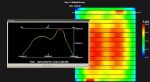
At the recent DesignCon 2020 in Santa Clara, Cadence introduced a new product, Sigrity Aurora. You won’t find a press release about this announcement. Rather, Brad Griffin, product management group director at Cadence, presented Sigrity Aurora in the theater at the Cadence booth. This one caught my eye and deserves some discussion.… Read More
I recently spent some time at DesignCon 2020 in Santa Clara. For those who haven’t attended this show in a while, you need to go. It’s no longer a small event focused on chip design. It has grown into a true system-level conference, with a broad ecosystem represented on the show floor and in the technical sessions. Ecosystem is an important… Read More


Flynn Was Right: How a 2003 Warning Foretold Today’s Architectural Pivot