You are currently viewing SemiWiki as a guest which gives you limited access to the site. To view blog comments and experience other SemiWiki features you must be a registered member. Registration is fast, simple, and absolutely free so please,
join our community today!
WP_Term Object
(
    [term_id] => 50
    [name] => Events
    [slug] => events
    [term_group] => 0
    [term_taxonomy_id] => 50
    [taxonomy] => category
    [description] =>
    [parent] => 0
    [count] => 1564
    [filter] => raw
    [cat_ID] => 50
    [category_count] => 1564
    [category_description] =>
    [cat_name] => Events
    [category_nicename] => events
    [category_parent] => 0
    [is_post] =>
)
The incredible growth that the semiconductor industry has enjoyed over the last several decades is attributed to Moore’s Law. While no one argues that point, there is also industry wide acknowledgment that Moore’s Law started slowing down around the 7nm process node. While die-size reductions still scale, performance jumps… Read More
My third event at DAC on Monday was all about using EDA tools in the Cloud, and so I listened to Craig Johnson, VP EDA Cloud Solutions, Siemens EDA. Early in the day I heard from Joe Sawicki, Siemens EDA, on the topic of Digitalization.
Why even use the Cloud for EDA? That’s a fair question to ask, and Craig had several high-level… Read More
Now that the 58th Design Automation Conference held this year in San Francisco has concluded, we take a minute to look back at the results and ascertain what it meant for our company.
Unfortunately, many popular tradeshows held in the time of Covid have suffered a drop in attendance, and DAC was no exception. Despite this however,… Read More
The Electronic Design Automation (EDA) industry used to be a bustling bazaar of scrappy startups, along with medium sized companies that dominated a technology space, and big main-line vendors. The annual Design Automation Conference was noisy, hectic, and sprawled over multiple large convention halls. This diversity meant… Read More
Top 10 Takeaways from DAC 2021by Tom Dillinger on 12-15-2021 at 2:00 pmCategories: Accellera, EDA, Events
The “in-person” portion of the Design Automation Conference (DAC) was recently held in San Francisco. (As several presenters were unable to attend, a “virtual” program is also available.) The presentations spanned a wide gamut – e.g., technical advanced in design automation algorithms; new features in commercial EDA tools; … Read More
- Semicon West was Semicon Less- Less Customers & Vendor
- Everyone is busy as can be, maybe too busy to attend
- Those who were there, talk about supply chain issues & stress
- How long does the party last & where the money comes from?
Semicon West was Semicon Less….
We attended a “Hybrid” version of Semicon… Read More
Functional safety has been at the forefront of the electrification of our vehicles with new ADAS features, and the push to reach autonomous driving, while having compliance with the ISO 26262 functional safety standard. I attended the Accellera hosted panel discussion on Monday at DAC, hearing from functional safety panelists… Read More
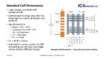
Standard Cell Scaling
Complex logic designs are built up from standard cells, in order to continue to scale logic we need to continually shrink the size of standard cells.
Figure 1 illustrates the dimensions of a standard cell.
Figure 1. Standard Cell Dimensions.
From figure 1 we can see that shrinking standard cell sizes requires… Read More
Monday at DAC this year started off on a very optimistic note as Joe Sawicki from Siemens EDA presented in the Pavilion on the topic of Digitalization, a frequent theme in the popular press because of the whole Work From Home transition that we’ve gone through during the pandemic. Several industries are benefiting from the… Read More
Thermal modeling has become a hot topic for designers of today’s high-speed circuits and complex packages. This has led to the adoption of better and more sophisticated thermal modeling tools and flows as exemplified in this presentation by Micron at the IDEAS Digital Forum. The presentation is titled “Thermal Aware Memory Controller… Read More


Podcast EP357: How Gonka is Changing the Way AI is Accessed with David Liberman