You are currently viewing SemiWiki as a guest which gives you limited access to the site. To view blog comments and experience other SemiWiki features you must be a registered member. Registration is fast, simple, and absolutely free so please,
join our community today!
WP_Term Object
(
    [term_id] => 50
    [name] => Events
    [slug] => events
    [term_group] => 0
    [term_taxonomy_id] => 50
    [taxonomy] => category
    [description] =>
    [parent] => 0
    [count] => 1522
    [filter] => raw
    [cat_ID] => 50
    [category_count] => 1522
    [category_description] =>
    [cat_name] => Events
    [category_nicename] => events
    [category_parent] => 0
    [is_post] =>
)
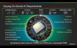
During his keynote address at the CadenceLIVE 2021 conference, CEO Lip-Bu Tan made some market trend comments. He observed that most of the data nowadays is generated at the edge but only 20% is processed there. He predicted that by 2030, 80% of data is expected to be processed at the edge. And most of this 80% will be processed on edge… Read More
The subject of this webinar is focused on the new COM-HPC standard from PICMG, a nonprofit consortium of companies and organizations that collaboratively develop open standards for high performance telecommunications, military, industrial, and general-purpose embedded computing applications. A computer-on-module … Read More
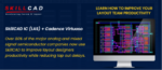
Originally containing a handful of commands to help with common layout tasks, SkillCAD has evolved into the industry standard for analog, RF and mixed signal design for customers using Cadence Virtuoso. With over 85 customers worldwide and over 120 functions including the powerful, patented V-editor, metal routing and pin… Read More
The GF Technology Summit was last week. It was virtual again this year but with a different format. It was a mix of live and recorded events which did include some cringe worthy moments but all-in-all it was well worth my time.
One of the biggest changes you will notice is the messaging. GF is no longer down in the technology trenches … Read More
I’ve attended the DAC conference and trade show since the late 1980s, and every visit has been a continuing learning experience about the EDA, IP and semiconductor industry. I first started attended as an EDA vendor in 1987, and since 2004 as a freelance marketing professional. There’s a significant amount of preparation… Read More
For those of you following the latest developments in electronic design it has become clear that the industry is transitioning through an inflection point that is shifting some of the ground rules of design. The increase in the speed and integration density in today’s systems are blurring the lines between chip design and system… Read More
Introduction
At the recent Intel Architecture Day presentations, a breadth of roadmap plans were provided – an earlier article focused on the x86 client and data center cores and products. This article focuses on the GPU and IPU announcements.
Xe Graphics Core
The Intel GPU architecture for embedded, discrete, and data center… Read More
Introduction
The optimization of computing throughput, data security, power efficiency, and total cost of ownership is an effort that involves managing interdependencies between silicon and packaging technologies, architecture, and software. We often tend to focus on the technology, yet the architecture and software… Read More
Everyone knows IP is an important asset for the enterprise. You spend a lot of money on IP licenses. You try to keep track of who bought what as buying the same thing twice is painful. You wonder if you have the latest version of an IP, especially if it’s part of mission-critical functionality. If you’re a good corporate citizen, you … Read More
DesignCon has grown over the years to become a true system design show. The show’s tagline is WHERE THE CHIP MEETS TO BOARD. This is just the beginning. Besides the chip and the board there are all the challenges, opportunities, and options to get signals reliably propagated throughout the entire system. Power, signal integrity,… Read More


Musk’s Orbital Compute Vision: TERAFAB and the End of the Terrestrial Data Center