It’s all around us. The pervasive use of AI is changing our world. From planetary analysis of weather patterns to monitoring your vital statistics to assess health, it seems as though smart everything is everywhere. Much has been written about the profound impact AI is having on our lives and society. Everyone seems to agree that… Read More

Webinar: Semifore Offers Three Perspectives on System Design Challenges
The exponential increase in design complexity is a popular topic these days. In fact, it’s been a topic of discussion for a very long time. The explosion of chip and system design complexity over the past ten years has become legendary and haunts many of us daily. A lot of the complexity we face has to do with coordinating across an ever-increasing… Read More
Why China hates CHIPS

The CHIPS and Science Act has its fair share of critics, with detractors calling it corporate welfare for “losers” like Intel, or lacking guardrails to prevent companies making legacy chips in China.
One of the most vocal opponents of the act has been China’s communist-ruled government.
WEBINAR: Intel Achieving the Best Verifiable QoR using Formal Equivalence Verification for PPA-Centric Designs
Synopsys Fusion Compiler offers advanced optimizations to achieve the best PPA (power, performance, area) on today’s high-performance cores and interconnect designs. However, advanced transformation techniques available in synthesis such as retiming, multi-bit registers, advanced datapath optimizations, etc. are
2022 Semiconductor Supercycle and 2023 Crash Scenario
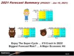
Charles Shi, semiconductor analyst at Needham & Company, an US-based investment bank and asset management firm, hosted an expert call on semiconductor cycles with Malcolm Penn, Founder and CEO of Future Horizons on 18 August 2022, with over 100 financial analysts in attendance. The following bulletin is a summary of the… Read More
Enhanced X-NAND flash memory architecture promises faster, denser memories
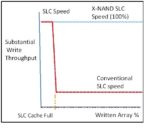
Although the high-performance X-NAND memory cell and architecture were first introduced in 2020 by Neo Semiconductor, designers at Neo haven’t rested on that accomplishment and recently updated the cell and the architecture in a second-generation implementation to achieve 20X the performance of conventional quad-level-cell… Read More
Getting Ahead with Semiconductor Manufacturing Equipment and Related Plasma Reactors
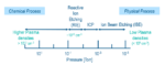
Advanced semiconductor fabrication technology is what makes it possible to pack more and more transistors into a sq.mm of a wafer. The rapidly increasing demand for advanced-process-based chips has created huge market opportunities for semiconductor manufacturing equipment vendors. According to SEMI, worldwide sales … Read More
EDA Product Mix Changes as Hardware-Assisted Verification Gains Momentum

The Design Automation Conference, as always, is a good barometer on the state of EDA and my area of interest, verification. The recent DAC offered plenty of opportunities to check on trends and the status quo.
Remarkably, exhibitors and attendees were upbeat about the chip design landscape despite concerns about supply chain … Read More
WEBINAR: A Revolution in Prototyping and Emulation

This webinar will introduce to you a revolutionary new way to do prototyping and emulation at best-in-class performance, productivity, and pricing by unifying the hardware and a new software stack so one system is capable of prototyping and delivering essential emulation functionality.
Register Here
The speed of Moore’s law… Read More
An EDA AI Master Class by Synopsys CEO Aart de Geus

I consider Dr. Aart de Geus one of the founding fathers of EDA and one of the most interesting people in the semiconductor industry. So it is not a surprise that Aart was chosen to attend the CHIPs Act signing at the White House.
Here is his current corporate bio:
Since co-founding Synopsys in 1986, Dr. Aart de Geus has expanded Synopsys… Read More
Musk’s Orbital Compute Vision: TERAFAB and the End of the Terrestrial Data Center