You are currently viewing SemiWiki as a guest which gives you limited access to the site. To view blog comments and experience other SemiWiki features you must be a registered member. Registration is fast, simple, and absolutely free so please,
join our community today!
WP_Term Object
(
    [term_id] => 50
    [name] => Events
    [slug] => events
    [term_group] => 0
    [term_taxonomy_id] => 50
    [taxonomy] => category
    [description] =>
    [parent] => 0
    [count] => 1516
    [filter] => raw
    [cat_ID] => 50
    [category_count] => 1516
    [category_description] =>
    [cat_name] => Events
    [category_nicename] => events
    [category_parent] => 0
    [is_post] =>
)
Now that the dust has settled with the Softbank acquisition I must say that Arm is truly a different company. There are now a lot of new faces from outside the semiconductor industry, which is a good thing, and a lot less stress from Wall Street which is an even better thing. Simon can now wear whatever he wants without the worry of lowering… Read More
This week Dr. Eric Esteve, Dr. Bernard Murphy, and I will be blogging live from Arm TechCon. It really looks like it will be a great conference so you should see some interesting blogs in the coming days. One of the topics I am interested in this year is foundation IP and I will tell you why.
During the fabless transformation of the semiconductor… Read More
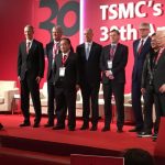
The TSMC 30th Anniversary Forum just ended so I will share a few notes before the rest of the media chimes in. The forum was live streamed on tsmc.com, hopefully it will be available for replay. The ballroom at the Grand Hyatt in Taipei was filled with cameras, semiconductor executives, and security personnel.
Here is the replay
The… Read More
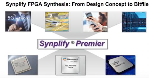
You might wonder why, in FPGA design, you would go beyond simply using the design tools provided by the FPGA vendor (e.g. Xilinx, Intel/Altera and Microsemi). After all, they know their hardware platform better than anyone else, and they’re pretty good at design software too. But there’s one thing none of these providers want to… Read More
“Mobile is the largest platform ever built by humanity”, Christiano Amon, Executive Vice President, Qualcomm Technologies, Inc. and President, Qualcomm CDMA Technologies speaking at the GLOBALFOUNDRIES Technologies Conference (GTC) 2017.… Read More
The 63rd annual IEDM (International Electron Devices Meeting) will be held December 2nd through 6th in San Francisco. In my opinion IEDM is one of, if not the premier conference on leading edge semiconductor technology. I will be attending the conference again this year and providing coverage for SemiWiki. As a member of the press… Read More
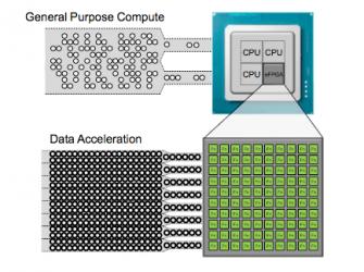
Accelerating compute-intensive software functions by moving them into hardware has a long history, stretching back (as far as I remember) to floating-point co-processors. Modern SoCs are stuffed with these applications, from signal processors, to graphics processors, codecs and many more functions. All of these accelerators… Read More
Next week is ARM TechCon which is one of my favorite conferences (SemiWiki is an event partner). This year is lucky number thirteen for ARM TechCon and it includes more than sixty hours of sessions plus more than one hundred ARM partners in the exposition. I will be signing free copies of our new book “Custom SoCs for IoT: Simplified”… Read More
Magillem is hosting a user group meeting on October 26th at The Pad in Sunnyvale. User Group meetings are always educational; this one should be especially so for a number of reasons, not least of which is the keynote topic: Expert Systems for Experts.
REGISTER HERE for the meeting in Sunnyvale on October 26[SUP]th[/SUP] from 10:00am… Read More
ANSYS and TSMC will be co-presenting at ARM TechCon on Multiphysics Reliability Signoff for Next Generation Automotive Electronics Systems. The event is on Thursday October 26th, 10:30am-11:20am in Grand Ballroom B.
You can get a free Expo pass which will give you access to this event HERE and see the session page for the event … Read More


Chemical Origins of Environmental Modifications to MOR Lithographic Chemistry