You are currently viewing SemiWiki as a guest which gives you limited access to the site. To view blog comments and experience other SemiWiki features you must be a registered member. Registration is fast, simple, and absolutely free so please,
join our community today!
WP_Term Object
(
    [term_id] => 50
    [name] => Events
    [slug] => events
    [term_group] => 0
    [term_taxonomy_id] => 50
    [taxonomy] => category
    [description] =>
    [parent] => 0
    [count] => 1516
    [filter] => raw
    [cat_ID] => 50
    [category_count] => 1516
    [category_description] =>
    [cat_name] => Events
    [category_nicename] => events
    [category_parent] => 0
    [is_post] =>
)
Welcome to my newly relocated column, I am so excited about my new relationship with Daniel Nenni, and the other esteemed bloggers on SemiWiki. For those who do not know me, I have been a featured columnist on another EDA portal for the past 12-plus years, and in EDA for 20-plus years. As the leading recruiter in our industry, (or so … Read More
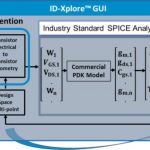
My IC design career started out with circuit design of DRAMS, so I got to quickly learn all about transistor-level design at the number one IDM in the world, Intel at the time. In the early days, circa 1978 we circuit designers actually had few EDA tools, mostly a SPICE circuit simulator followed by manual extraction, manual netlisting,… Read More
Getting your tape-out done on time is hard, but can it be made easier? That was the main topic of Mentor’s Calibre Panel held at DAC 2018, attended by a few key players in IC design ecosystem: Bob Stear, VP of Marketing at Samsung represented the foundry side; from the IP side, Prasad Subramaniam, VP of eSilicon for R&D and Technology;… Read More
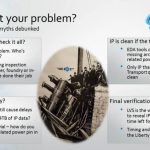
This year I signed books in the Fractal booth (compliments of Fractal) and let me tell you it was quite an experience. IP quality is a very touchy subject and the source of many more tape-out delays than I had imagined. As it turns out, commercial IP is the biggest offender which makes no sense to me whatsoever. Even more shocking, one… Read More
A chain is as strong as its weakest link. This phrase resonates well in Static Timing Analysis (STA) domain, though it is about accuracy rather than durability. As timing signoff step provides the final performance readings of a design, an STA outcome is as good as its underlying components. Aside from the parasitic extraction … Read More
Driving into DAC on Sunday afternoon was a chore since Gay Pride week was finishing with the Gay Pride Parade. Streets were closed, traffic was crazy, and people were roller skating naked which seems wrong on so many levels. This year the opening ceremonies were in the convention center hallway which also seemed wrong. Long lines… Read More
DAC 2018 Potpourriby Alex Tan on 07-03-2018 at 12:00 pmCategories: Arm, EDA, Events, RISC-V
The venue
Despite of being held at the new three-story Moscone West building, this year 55th DAC in San Francisco bore many similarities as compared with last year’s. Similar booth decors and floorplan positioning of the big two, Synopsys and Cadence, which were across of each other and right next to the first floor entrance –although… Read More
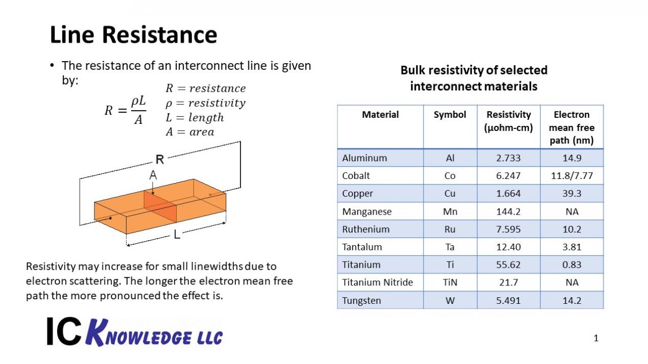
The IEEE Interconnect Technology Conference (IITC): Advanced Metallization Conference was held June 4th through 7th in Santa Clara. Imec presented multiple papers on comparing copper, cobalt and ruthenium interconnect. One paper in particular caught my eye: Marleen H. van der Veen, # N. Heylen, O. Varela Pedreira, S. Decoster,… Read More
This was my 35th DAC and it did not disappoint, especially when it came to the DAC Drama Department. This year DAC proved once again that it is THE place for semiconductor professionals and academics to learn and network. The big news is that Synopsys did not reserve a booth for 56DAC in Las Vegas next year which resulted in quite a bit… Read More
The second keynote at Mentor’s U2U this year was given by Hooman Moshar, VP of Engineering at Broadcom, on the always (these days) important topic of design for power. This is one of my favorite areas. I have, I think, a decent theoretical background in the topic, but I definitely need a periodic refresh on the ground reality from the… Read More


Captain America: Can Elon Musk Save America’s Chip Manufacturing Industry?