Next week is the SPIE Advanced Lithography Conference in San Jose, the premier conference for advanced lithography used to produce state-of-the-art semiconductors. Last year I blogged after the conference about some of the key points I heard at the conference and this year I plan to do the same.

Electronic Design Automation
Synopsys Earnings Call Q1 2015

Synopsys announced their results yesterday. Their 2014 already ended, this is the end of their fiscal first quarter. On the call were Aart, one of Synopsys’s two co-CEOs, the other being Chi-Foon Chan; and Trac Pham, the new CFO on his first earnings call.
Synopsys’s results were good. A quick look at the results. Revenue was $542M… Read More
FinFET Designs Need Early Reliability Analysis
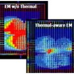
In a world with mobile and IoT devices driven by ultra-low power, high performance and small footprint transistors, FinFET based designs are ideal. FinFETs provide high current drive, low leakage and high device density. However, a FinFET transistor is more exposed to thermal issues, electro migration (EM), and electrostatic… Read More
Mentor and ASSET Intertech Do a DFT World Tour
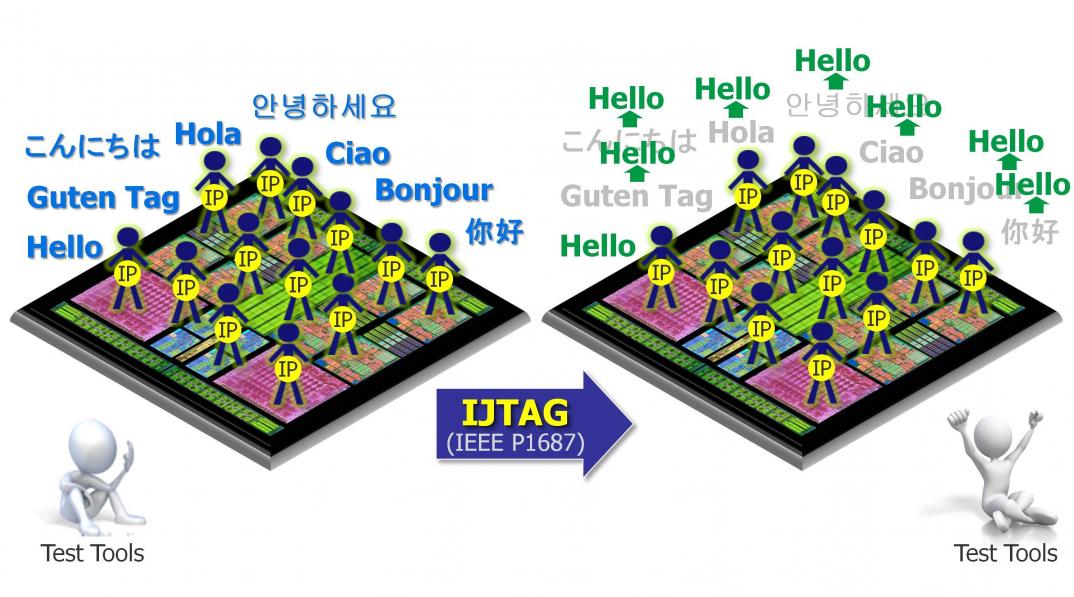
The Mentor Graphics test folks and ASSET Intertech have teamed up to provide a series of free DFT seminars in the US, Europe, and Asia. The first one is in Austin, TX on February 19, 2015, and the last is in Tokyo on April 24. Hereis the full list of locations and dates.
The morning session covers IJTAG. The new IEEE 1687 Internal JTAG (IJTAG)… Read More
Mentor shows post-PC industrial device approach
The term “human machine interface” originated from the factory floor. In the context of HMI, machine refers not to the computer, but to a machine tool or other instrument the computer was attached to. For decades, if an HMI was needed, it was implemented on a PC or single-board computer running Microsoft Windows. Real-time processing… Read More
MEMS Require 3D Field Solver for Accurate Cap Values

MEMS devices have become extremely important and common. Freescale last year reported its combined MEMS shipments exceeded 2 billion units. If we just examine how many accelerometers we each probably own today, it is easy to see why the market for these products is growing so rapidly. The first and most obvious device is our cell… Read More
Physically Aware DFT Improves PPA
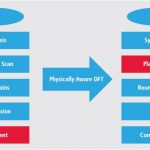
Introducing on-chip test circuitry has become a necessary criteria for an ASIC’s post manufacture testability. The test circuitry is usually referred as DFT (Design-for-Test) circuit. A typical methodology for introducing DFT circuit in a design is to replace usual flip-flops with special types of flip-flops called ‘scan… Read More
Secure Processor for IoT
In my last blog “Processor for IoT” I have discussed security as one of the key requirements for processor used in IoT devices. In this blog we will analyze different method of hacking and some techniques which can be used to prevent those security breaches.
One of the common ways of attack is to probe address and data … Read More
Do You Need a Silicon Catalyst?

Lately there has been significant concern over the rising costs of designing in silicon and the troubling decline in venture investments in semiconductors. These alarming trends include fewer IPOs, a falloff in the amount and frequency of early stage seed investments, and comparatively low industry organic growth rates. A … Read More
More Test Points are Better
I got really involved in testability back at CrossCheck in the 1990’s when they designed a way for Gate Arrays to have 100% observability without any Design For Test (DFT) requirements on designers. The Japanese Gate Array companies loved this approach and their customers enjoyed the highest test coverage without being… Read More
Enhancing Multi-Domain System Simulation with FMI Co-Simulation