You are currently viewing SemiWiki as a guest which gives you limited access to the site. To view blog comments and experience other SemiWiki features you must be a registered member. Registration is fast, simple, and absolutely free so please,
join our community today!
WP_Term Object
(
    [term_id] => 157
    [name] => EDA
    [slug] => eda
    [term_group] => 0
    [term_taxonomy_id] => 157
    [taxonomy] => category
    [description] => Electronic Design Automation
    [parent] => 0
    [count] => 4439
    [filter] => raw
    [cat_ID] => 157
    [category_count] => 4439
    [category_description] => Electronic Design Automation
    [cat_name] => EDA
    [category_nicename] => eda
    [category_parent] => 0
    [is_post] =>
)
IC Design at ZMDIby Daniel Payne on 11-28-2014 at 7:00 pmCategories: EDA, Perforce
As a blogger I have the privilege of meeting many IC designers from around the world, mostly through contact on LinkedIn or from connecting at trade shows. Through a contact at DACI met up with Achim Graupner, a manager of methodology and design automation from ZMDI, then asked him for an interview to understand how his group does … Read More
In today’s electronics with multiple functions working together, heat generation is on the rise; sometimes it becomes intolerable. In fact components running at different temperatures can cause timing issues, and very high temperatures can lead to operational issues such as latch-up. An electronic system can contain chips,… Read More
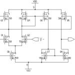
There’s much talk in EDA about High Level Synthesis (HLS), Transaction Level Modeling (TLM) and the Universal Verification Methodology (UVM), however there’s a lower-level of abstraction, the transistor-level, where high-speed digital cell libraries are created, analog circuits are crafted, and AMS designers… Read More
The simple answer is when everything in the world is smart. But if you think deeply, you would find that the continuous progression to make things easy in life is what makes the world smarter day-by-day – the sky is the limit. In the world of computing, consider the 17[SUP]th[/SUP] century era when humanbrain was used as a computer … Read More
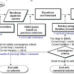
Ad hoc digital design verification approaches ran out of steam at least a decade ago when designs got intractably large to make it feasible to keep track of everything with pen and paper and excel. But analog design has remained largely ad hoc to this day. The designer runs spice, looks at the waveforms that come out and decide whether… Read More
Getting a printed circuit board from design and into production presents one of the biggest challenges in successfully launching a product. The designer’s job is to anticipate issues that can adversely affect PCB fabrication and assembly. Design rules and component libraries go part of the way, but there is a thicket of things… Read More
At ARM TechCon I ran into Coby Hanoch who has just been appointed VP worldwide sales of a comany that I’d not previously heard of called Codasip. As the name implies they supply code, and ASIPs. Well, actually IP source code and ASIP tools. The company is based in Brno (pronounced pretty much like Bruno) in the Czech republic … Read More
Two weeks ago I blogged about amorphous silicon and how that material is well-suited for designing TFTs. Today I’m following up after watching the archived webinarpresented by Nam-Kyun Tak of Silvaco. After clicking on that link you’ll be brought to a brief sign-up page and then can watch the archived webinar in your… Read More
For about a decade I am looking forward to seeing more of system level design and verification including high level synthesis (HLS), virtual prototyping, and system modeling etc. to come in the main stream of SoC design. Although the progress has been slow, I see it accelerating as more and more tools address the typical pain points… Read More
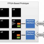
Debugging an ASIC design in an FPGA-based prototyping system can be a lot like disciplining a puppy. If you happen to be there at the exact moment the transgression occurs and understand what led up to that moment, administering an effective correction might be possible.
Catching RTL in the act requires the right tools. Faults in… Read More


Silicon Insurance: Why eFPGA is Cheaper Than a Respin — and Why It Matters in the Intel 18A Era