You are currently viewing SemiWiki as a guest which gives you limited access to the site. To view blog comments and experience other SemiWiki features you must be a registered member. Registration is fast, simple, and absolutely free so please,
join our community today!
TSMC and Synopsys hosted a webinar in December on this topic of double patterning and how it impacts the IC extraction flow. The 20nm process node has IC layout geometries so closely spaced that the traditional optical-based lithography cannot be used, instead lower layers like Poly and Metal 1 require a new approach of using two… Read More
I’ve taught Verilog classes and used logic synthesis tools for ASIC and FPGA designs, so was interested to hear about Oasys Design Systems. I attended their webinar at 9AM today, so I’ll share what I learned about their approach to logical and physical synthesis. This approach competes with tools like Design Compiler… Read More
This morning I spoke with Mahesh Tirupattur, Executive VP of Analog Bits about IC design challenges and using EDA tools to create high performance, mixed-signal semiconductor IP.
… Read More
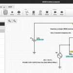
I love all things SPICE so when I read a tweet tonight from @PartSimI just had to try out their Schematic Capture and SPICE circuit simulator in a browser. The site is www.partsim.com and all you need is a web browser and short registration process, then it’s off to the Examples where I found a simple CMOS inverter and then extended… Read More
Last month the folks at Tektronix did something very useful, they invited 30 engineers to talk directly with their chief engineer of embedded instrumentation as part of “Meet the Experts” in Santa Clara, CA.
Brad Quinton, Chief Architect created a new and efficient approach of embedding instrumentation in your … Read More
In November and December I upgraded three devices and share my opinions on the utility of each:
- Samsung Galaxy Note (aka Phablet = Phone + Tablet)
- Kindle Paperwhite (e-reader)
- Google Nexus 7 (Tablet)
…
Read More
Design For Manufacturing (DFM) is the art and science of making an IC design yield better in order to receive a higher ROI. Ian Smith, an AE from Mentor in the Calibre group presented a pertinent webinar, IP Scoring Using TSMC DFM Kits. I’ll provide an overview of what I learned at this webinar.… Read More
In 2012 FinFET is one of the most talked about MOS technologies of the year because traditional planar CMOS has slowed down on scaling below the 28nm node. To learn more about FinFET process modeling I attended a Synopsys webinar where Bari Biswas presented for about 42 minutes include a Q&A portion at the end.
Bari Biswas, Synopsys… Read More
An email update from John Cooley at DeepChip this morning prompted the bloggers here at SemiWiki to continue the discussion and point out incorrect data, so that readers realize what is really happening with our media portals as sources of timely and relevant news and opinion. I respect what John Cooley has done with DeepChip over… Read More
At DAC in June I first blogged about Symicabecause they offered a Fast SPICE circuit simulator, and today I discovered a free version so I decided to write up a mini-review for you.… Read More


Intel 18A vs Intel 18A-P: What Is the Difference and Why Does It Matter?